
Suk Lee drew the short straw at the TSMC Symposium yesterday, with the 5pm slot. Not only late in the day but between all the attendees and free beer. The morning sessions had been standing room only, with several hundred standees (as they call them on muni around here, but isn’t a standee really someone being stood on?). But through the day numbers dwindled and the late afternoon sessions were not well-attended.
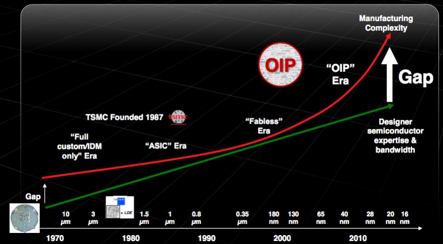
Suk started off with a little history of semiconductor. In the beginning there was a huge gap between what electronic companies wanted and the semiconductor and design expertise they had. Semiconductor expertise was entirely inside the few IDMs (although we didn’t call them that back then). Then ASIC companies came along, such as LSI Logic (where Suk worked) and VLSI Technology (where I did). We made it possible for people with no deep semiconductor knowledge to design their own chips. So the gap between what the people wanting the chips and the stuff the manufacturers knew started to close. TSMC was founded in 1987 ushering in the foundry era, and even physical design and circuit design moved out to system companies. The EDA industry came into existence. The gap closed.
But in the current era, it has opened up again. There is just too much to know. Plus design is more and more IP-based. Most companies, even if they wanted to design their own DDRx PHY (why would you?) don’t have the knowledge, for example. Another change is that the highest volume market is mobile. It ramps fast and then it’s on to the next node. So the mobile (and other markets, to be sure) designs need to tapeout before the process is completely stable. There is no point in building a multi-billion dollar fab in just a few months, hand out the design rules, and then have it sit idle while mobile companies design their chips.
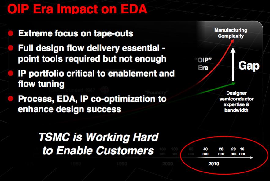
So TSMC’s Open Innovation Platform (OIP) is a way to close that gap and acknowledge that tools, libraries, key IP and everything need to come together at the finish line just as the process is ready to ramp to volume. It is no longer possible even for a huge fabless semiconductor company to have all the knowledge they need, nor for the tool vendors to take their time since every process generation we can see looking forward, starting with 28nm, has a huge discontinuous feature. You can’t design 20nm without tools that understand double patterning. You can’t design 16nm without tools that understand FinFET. 10nm has more complex patterning rules, since it requires self-aligning double patterning and cut masks. I’ve no idea what 7nm needs and probably there are things nobody knows yet.
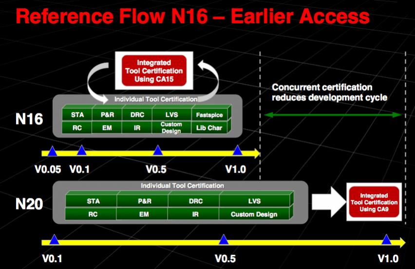
So OIP has to get a full reference flow together and delivered to early adopters much earlier than in the past. N20 (20nm) was faster than ever before but N16 (16nm) needs to be even faster.
OIP is a typical marketing name that doesn’t directly mean very much, but the reality is that getting designs to hit the fab when it is ready requires doing a lot of things much earlier than ever before. TSMC has been working with ARM for years, but more recently (again driven by mobile) they have started working with Imagination too.


The Packaging PDK Is the Missing Layer for Co-Packaged Optics