You are currently viewing SemiWiki as a guest which gives you limited access to the site. To view blog comments and experience other SemiWiki features you must be a registered member. Registration is fast, simple, and absolutely free so please,
join our community today!
For several decades now consumers like me have enjoyed using mobile devices including:
- Transistor radios, my first one had just 6 discreet transistors in the 1960’s
- HP 21 Calculator, used in college with Reverse Polish Notation, circa 1976
- Zenith Data Systems laptop, with two floppy drives, 1980’s
- Palm Pilot V,
…
Read More
IC designers have been creating with hierarchy for years to better manage large design sizes, however for the test world the concept of hierarchy and emerging standards is a bit newer. TSMC and Synopsys jointly created a webinarthat addresses hierarchical test, so I’ve attended it this week and summarized my findings here.… Read More
What do nVidia, Freescale and GlobalFoundries have in common? They are semiconductor companies? They are ARM licensees? They are doing 28nm chips? They all have the letter ‘a’ in their names?
All true, but that’s not what I was thinking of. But the letter ‘a’ is a clue since Apache (and Ansys) begin with ‘a’. All three companies have… Read More
Increasingly, SoC designs consist of assembling blocks of pre-designed IP. One special case is the derivative design where not just the IP blocks get re-used but a lot of the assembly itself. For example, in the design below some blocks are added, some blocks are updated, some hierarchy is changed. But the bulk of the design remains… Read More
There’s never a dull moment in the foundry race to offer FinFET processes that enable leading-edge SoC design. Today I attended a webinar hosted by Samsung and Synopsys on how to enable 14nm FinFET design. The two speakers were Dr. Kuang-Kuo Lin from Samsung and Dr. Henry Sheng from Synopsys.
Dr. Kuang-Kuo Lin, Samsung
Dr.… Read More
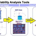
As we get down to smaller and smaller process nodes, the problem of soft errors becomes increasingly important. These soft errors are caused by neutrons from cosmic rays, alpha particles from materials used in manufacture and other sources. For chips that go into systems with high reliability this is not something that can be ignored.… Read More
Every process node these days has a new “gotcha” that designers need to be aware of. In some ways this has always been the case but the changes used to be gradual. But now each process node has something discontinuously different. At 20nm the big change is double patterning. At 14/16nm it is FinFET.
Rahul Deokar and John… Read More
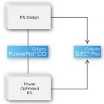
Sequential clock gating offers more power savings that can be obtained just with combinational clock gating. However, sequential clock gating is very complex as it involves temporal analysis over multiple clock cycles and examination of the stability, propagation, and observability of signal values.
Trying to do sequential… Read More
EDA vendors, IP suppliers and Foundries provide an eco-system for SoC designers to use in getting their new electronic products to market quicker and at a lower cost. An example of this eco-system are three companies (TSMC, Atrenta, Sonics) that teamed up to produce a webinar earlier in March called: Unlocking the Full Potential… Read More
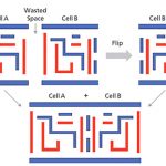
Design For Manufacturing (DFM) is the art and science of making an IC design yield better in order to receive a higher ROI. Ian Smith, an AE from Mentor in the Calibre group presented a pertinent webinar, IP Scoring Using TSMC DFM Kits. I’ll provide an overview of what I learned at this webinar.… Read More


