On Thursday July 9 Imec held a virtual technology forum. Imec is one of the premier research organizations working on semiconductor technology and their forums are always interesting. My area of interest is process technology and the following are my observation in that area from the forum.
Luc Van Den Hove
Luc Van Den Hove is the President and CEO of Imec and he led off the forum with an overview of the role of technology in the world today and Imec’s work.
For several years Design Technology Co Optimization (DTCO) has enabled continued scaling even as dimensional scaling has slowed. With DTCO process optimization has been realizing reduced track heights for standard logic cells. The height of a standard cell is the metal 2 pitch (M2P) multiplied by the number of tracks with a 6 track cell representing the current state-of-the-art.
In his presentation Luc outlined a roadmap with 6 track FinFETs giving way to 5 track nanosheets with buried power rails, then the addition of forksheets to enable 4.5 track nanosheets, to a 4 track CFET and eventually CFETs with 2D channels.
He also highlighted the need for Power, Performance, Area and Cost (PPAC). For many years leading edge logic process have been characterized based on Power, Performance and Area (PPA). For example, on recent conference calls TSMC has discussed their 3nm process as offering approximately 70% higher logic density, 10-15% higher speed at the same power or 25-30% lower power at the same performance. There is a growing realization that cost is an essential element of new process definition.
Authors note: I find this particularly interesting because in addition to blogging for SemiWiki I run IC Knowledge LLC, the world leader in cost modeling for Semiconductors and MEMS. Initial process definition in development occurs in a virtual environment these days with PPA all simulated before silicon is ever run. We have a product in beta testing that works in conjunction with process simulators to provide detailed cost estimates for process flows. We have already seen examples where high cost process steps were identified and mitigated before silicon was ever run.
Martin van den Brink
Martin van den Brink, the President and CTO of ASML presented the latest updates on ASML lithography.
There was lot of interesting information in his presentation, ASML consistently produces high-quality marketing slides.
He discussed their strategic investments to continue to move lithography forward and their holistic lithography approach to produce the desired image in a film on the wafer.
Some key points to me were immersion lithography productivity has increased by over 2x in the last 9 years, see figure 1.
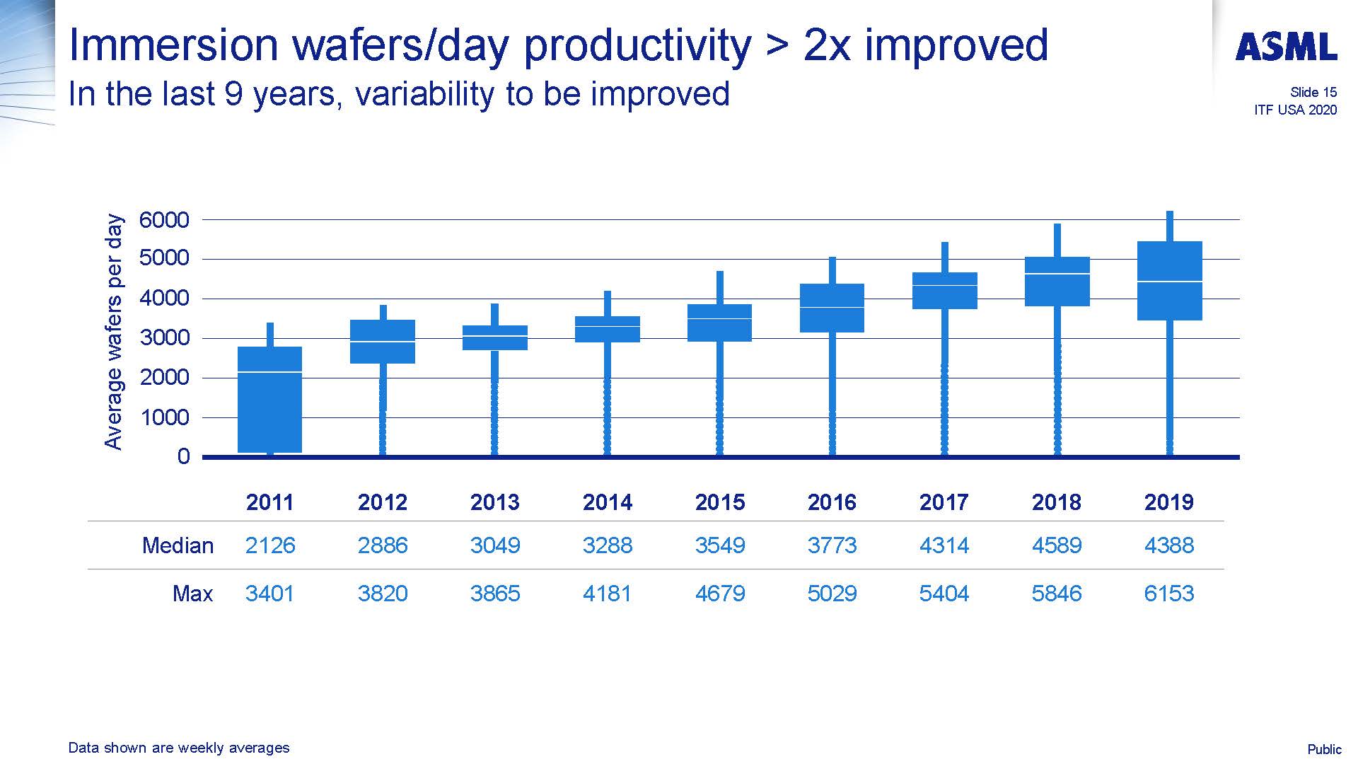
Figure 1. Immersion wafers per day versus year.
ASML has plans to improve the wafers per hour of all their optical exposure tools.
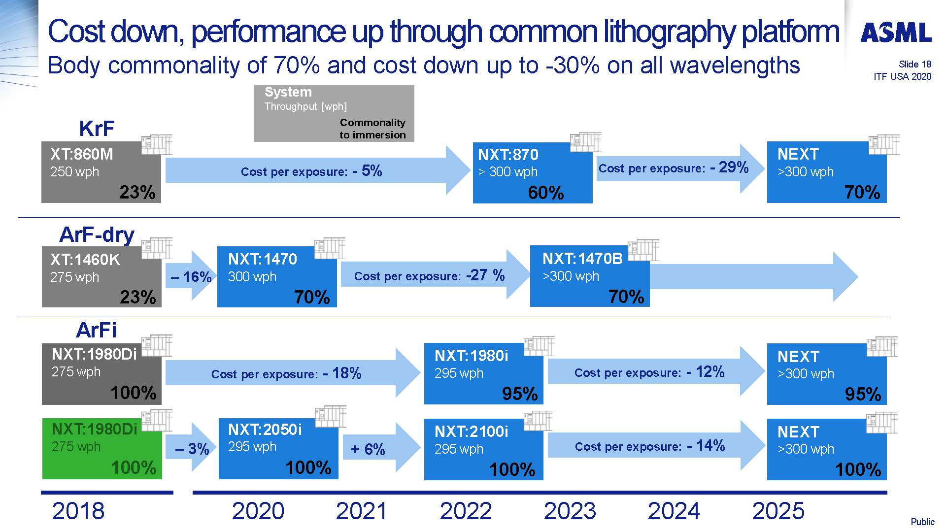
Figure 2. Improving throughput for optical exposure.
EUV continues to ramp up in production at ASML’s customers with over 11 million EUV wafers exposed and 57 3400x EUV system shipped (the 3400 platform is the EUV production platform).
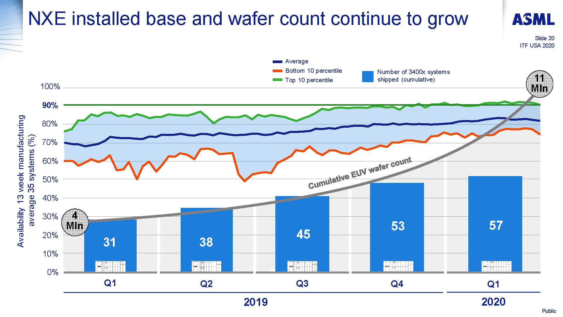
Figure 3. EUV installed base and wafers processed.
ASML has a plan to continue to drive up EUV throughput while reducing total energy per wafer. The 2x energy reduction in particular caught my attention and was new to me. They also expect to get 30mj/cm2 dose throughput up to 225 wafers per hour with the NXE3800 system!
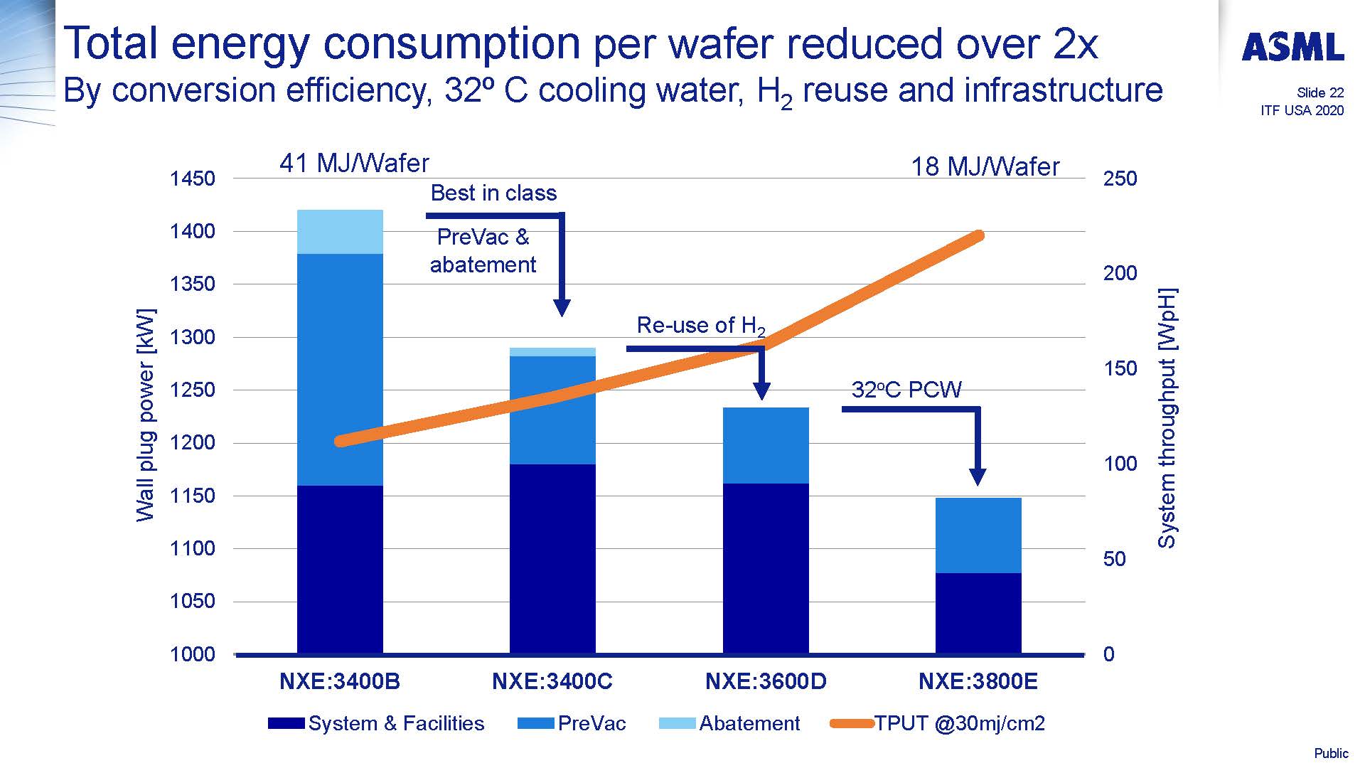
Figure 4. EUV throughput and power improvements.
There was also updates on resist development and the continuing progress on high NA EUV.
Sri Samavedan
Sri Samavedan, Senior Vice President of CMOS Technologies at Imec gave an update on Imec’s advanced semiconductor technology development.
As logic scaling continues to 3nm and below EUV will have to transition to multi-patterning until high NA EUV is available.
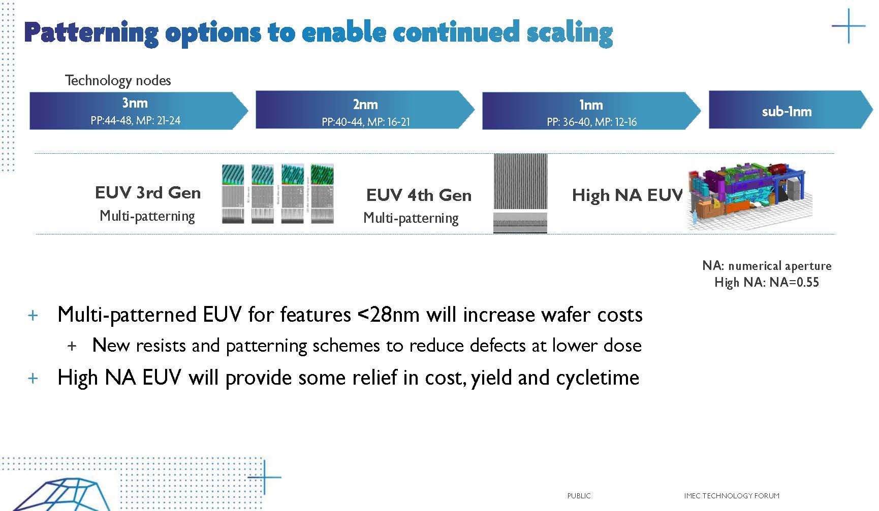
Figure 5. Lithography roadmap.
He also presented a logic scaling roadmap similar to the one in Luc Van Den Hove’s presentation but with additional details, for example to get to a 5 track cell the power rails need to be moved into the substrate as Buried Power Rails (BPR).
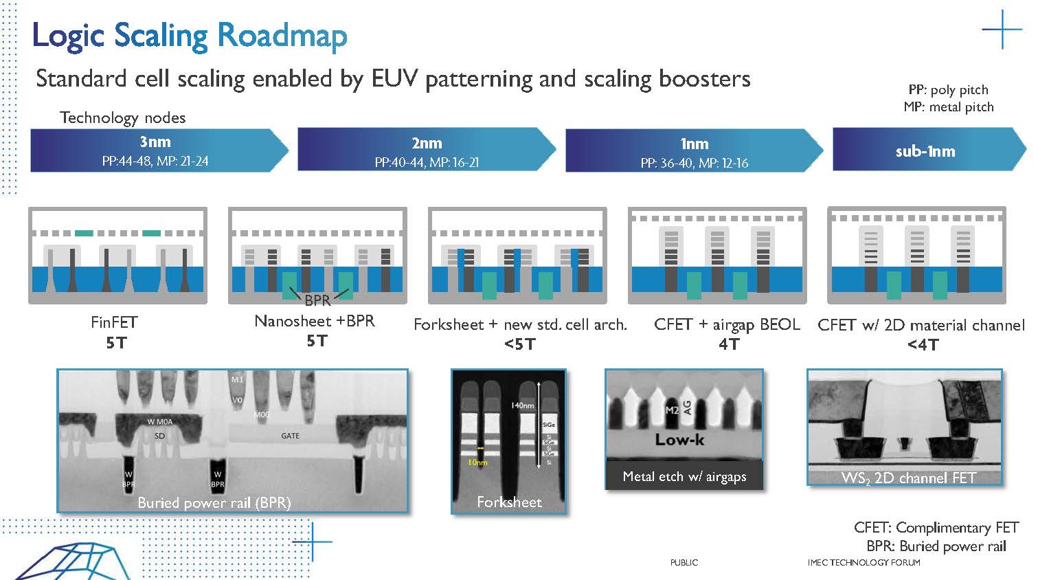
Figure 6. Logic scaling roadmap.
In 3D NAND one of the key challenges is how to continue to add more layers productively. As the stack gets taller patterning it gets harder and slower. Imec has been looking at Ruthenium (Ru) as a replacement for Tungsten (W) for the horizontal word line sheets. With Ru Imec believe they can get to approximately 15nm thickness for the world line sheet from the current approximately 30nm thickness. Personally, I think Ru is far too expensive to be implemented in 3D NAND but the concept of alternative materials is important.
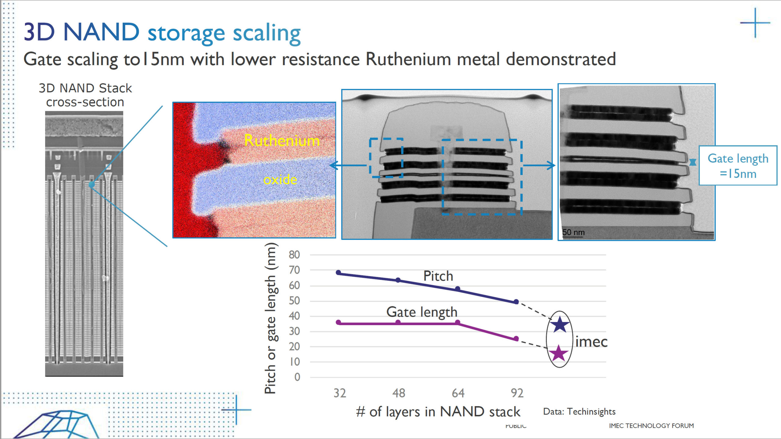
Figure 7. 3D NAND with Ru word lines.
He also talked about 2D Materials for logic and provided some data on MoS2 that can enable thinner channels and shorter channel lengths.
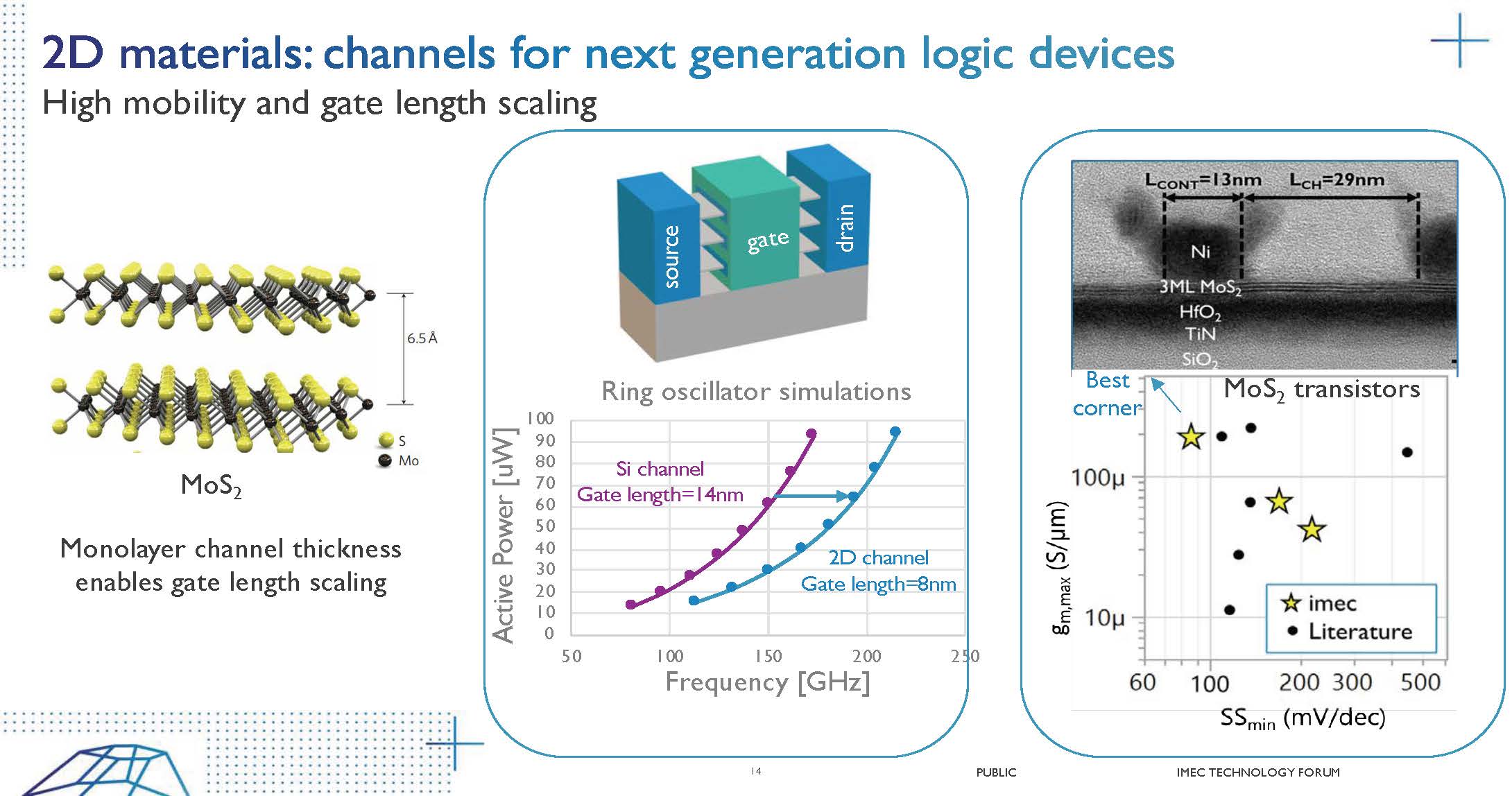
Figure 8. 2D channel materials.
Finally, I found the option of low temperature deposited Indium-Gallium-Zinc-Oxide (IGZO) for DRAM interesting. Of the three main semiconductor product areas, logic, NAND and DRAM, DRAM is facing the most unknown/difficult scaling challenge. A low temperature deposited low leakage transistor could enable stacking of both the access transistor and capacitor over the peripheral logic increasing DRAM density.
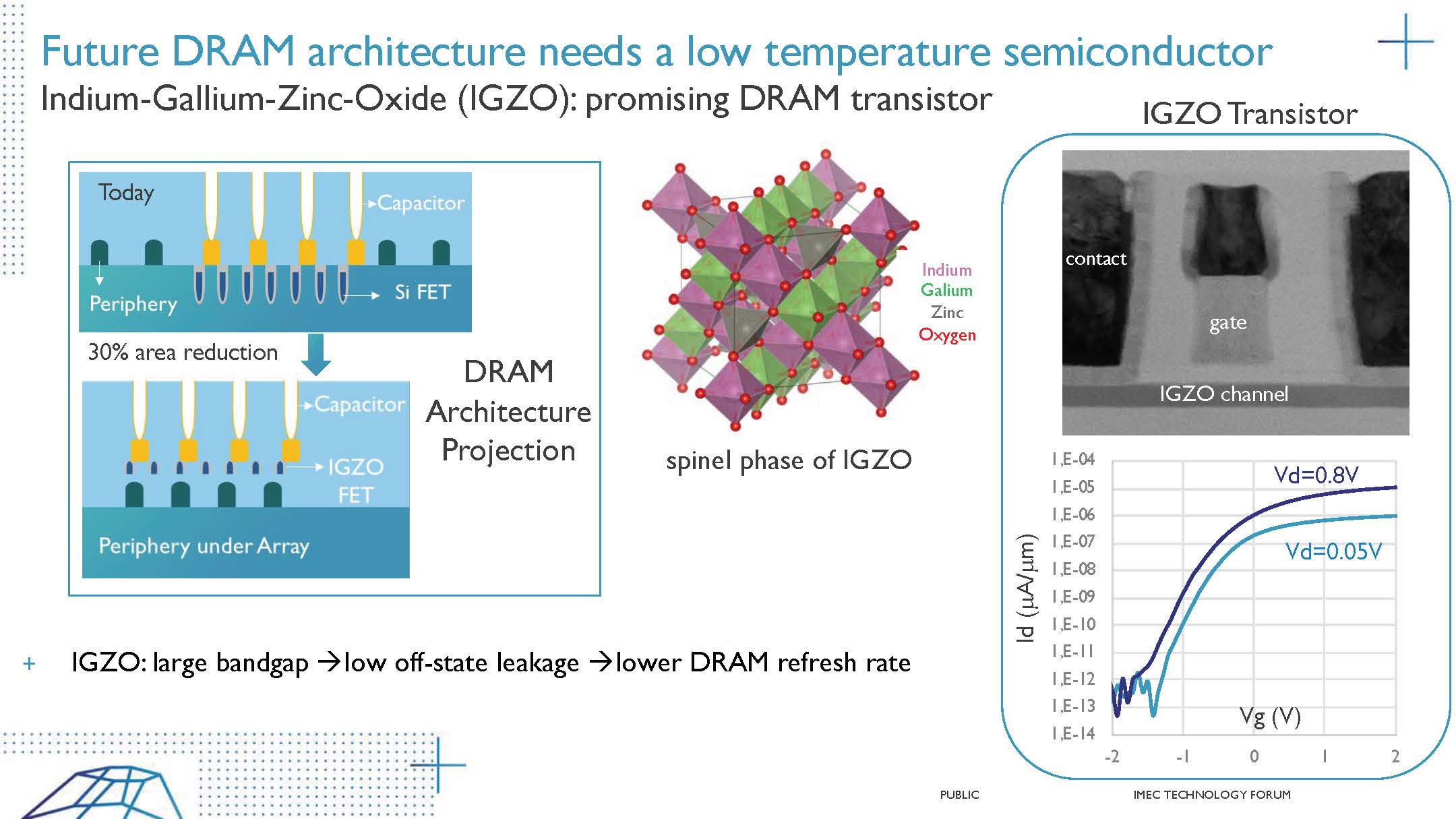
Figure 9. DRAM low temperature access transistor.
Conclusion
Imec and their development partners such as ASML continue to find solutions to drive semiconductor technology for many more years.
Also Read:
VLSI Symposium 2020 – Imec Buried Power Rail
Key Semiconductor Conferences go Virtual
Effect of Design on Transistor Density
Share this post via:


Comments
3 Replies to “Imec Technology Forum and ASML”
You must register or log in to view/post comments.