TSMC CoWoS versus Intel EMIB Semiconductor Packaging

TSMC CoWoS versus Intel EMIB Semiconductor Packaging
by Daniel Nenni on 07-17-2026 at 8:00 am

TSMC CoWoS verus Intel EMIB

There has been talk at the latest conferences about TSMC customers taking wafers to Intel for packaging. The question is why? Is it competitive pricing? Capacity? Supply chain diversity? CC Wei was asked about this during the last investor call and his perfect response was:

Jeff Su: I guess very simply put, EMIB-T, in his view, is gaining traction, how do we see the competitive threat from this?

C.C. Wei: Well, let me say that our packaging capacity is so tight that now it’s limiting my customers’ growth. We welcome that additional flexibility in the market. That will help TSMC’s front-end wafer business growth, which is a majority part of TSMC’s business. The technology looks good, according to the newspaper. We hope they will be successful, that share some of the loading from TSMC. Today, we’re working very hard to shorten the gap between the demand and the capacity. As I said, we welcome have this additional alternative, the flexibility for my customer.

What is the difference between TSMC CoWoS and Intel EMIB?

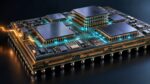
TSMC CoWoS and Intel EMIB are advanced packaging platforms designed to overcome the economic and physical limits of monolithic system-on-chip scaling. Both enable heterogeneous integration of logic, memory and specialized chiplets within one package, but they use fundamentally different interconnect structures. CoWoS generally creates a broad, high-density interconnect plane beneath the dies, whereas EMIB places small silicon bridges only where adjacent dies require dense communication. This architectural distinction drives differences in bandwidth distribution, package scaling, cost, thermal behavior and design methodology.

CoWoS, meaning Chip-on-Wafer-on-Substrate, is part of TSMC’s 3DFabric portfolio and is widely associated with high-performance computing and artificial-intelligence processors. In CoWoS-S, logic dies and high-bandwidth memory stacks are mounted on a passive silicon interposer containing fine-pitch wiring and through-silicon vias. The interposer is subsequently attached to an organic package substrate. Because almost the entire area under the active dies can provide dense routing, CoWoS-S supports extremely wide parallel interfaces, predictable signal paths and substantial die-to-die connectivity. TSMC states that CoWoS-S supports interposers up to approximately 3.3 reticles, or 2,700 square millimetres, while CoWoS-L and CoWoS-R support larger systems.

The CoWoS family is broader than a single silicon-interposer process. CoWoS-R replaces the large silicon interposer with a multilayer redistribution-layer interposer, reducing dependence on a complete sheet of interposer silicon. CoWoS-L combines an RDL-based interposer with localized silicon interconnect elements in regions requiring greater routing density. These variants allow designers to trade maximum wiring density against package size, cost and manufacturing complexity. Consequently, comparing EMIB only with CoWoS-S understates TSMC’s architectural flexibility. CoWoS-L, in particular, uses localized silicon structures that partially resemble bridge-based packaging. Both CoWoS-R and CoWoS-L entered volume production before or during 2024.

Intel’s Embedded Multi-die Interconnect Bridge embeds small passive silicon bridges inside an organic package substrate. Microbumps connect the edges of neighbouring dies to fine-pitch wiring on each bridge, while conventional substrate traces carry lower-density signals elsewhere. EMIB therefore avoids a package-wide silicon interposer and its associated through-silicon vias. Intel positions EMIB for logic-to-logic and logic-to-HBM integration and reports high-volume production use since 2017. Newer options include EMIB-M, which incorporates metal-insulator-metal capacitance, and EMIB-T, which adds through-silicon vias to the bridge for enhanced vertical connectivity and power delivery.

From an electrical perspective, CoWoS-S offers the most uniform high-density routing environment. A large interposer can distribute thousands of short connections among a central accelerator, multiple HBM stacks and additional chiplets without limiting dense links to die edges facing a bridge. This characteristic is especially valuable when broad connectivity is required across much of the package. The continuous interposer also permits designers to integrate power-distribution structures and decoupling capacitance close to active devices.

EMIB is more silicon-efficient when communication is localized between adjacent dies. It provides short, dense interconnections without paying the silicon-area cost of an interposer beneath components that do not require fine-pitch routing. However, complicated topologies may require multiple bridges, careful chiplet floorplanning and additional organic-substrate traces between nonadjacent components. The package architecture must align bridge locations precisely with the edges and interfaces of each die.

Mechanical and manufacturing trade-offs are similarly nuanced. Eliminating a large silicon interposer can reduce material usage and some wafer-processing operations, giving EMIB potential cost and yield advantages for appropriate designs. Its organic substrate remains difficult to manufacture because bridges must be embedded, planarized and aligned accurately. CoWoS-S adds a large, thin silicon structure whose fabrication, handling, warpage control and known-good-die assembly increase process complexity. Nevertheless, its regular interposer provides a mature and predictable routing platform. CoWoS-R and CoWoS-L attempt to reduce the size, cost and manufacturability constraints of full silicon interposers.

Neither architecture automatically solves heat removal. Both place high-power logic and HBM stacks in close proximity, increasing thermal coupling and local heat density. CoWoS can accommodate large logic-and-memory arrays, but package warpage, power delivery and cooling become harder as the interposer and package expand. EMIB permits relatively flexible die placement and avoids a continuous silicon layer, although thermal performance still depends principally on die power, spacing, heat-spreader design, package materials and system-level cooling.

Both technologies can also support vertical integration. Intel combines EMIB with Foveros die stacking to produce EMIB 3.5D systems containing multiple horizontally and vertically integrated chiplets. TSMC can combine CoWoS with its SoIC wafer-level stacking platform. These combinations allow designers to place cache, logic or specialized functions vertically while using CoWoS or EMIB for package-level horizontal connectivity.

The practical selection criterion is therefore connectivity geometry rather than a simple performance ranking. CoWoS-S is strongest when a system requires a large, continuous and extremely dense interconnect fabric, particularly between accelerators and multiple HBM stacks. CoWoS-R and CoWoS-L extend this approach toward larger or more cost-conscious products. EMIB is strongest when high-bandwidth links are concentrated at particular die boundaries and designers value silicon efficiency, modularity and avoidance of a full interposer.

Bottom line: CoWoS emphasizes an interposer-centric system fabric, while EMIB emphasizes localized silicon bridges embedded in an organic substrate. The better choice depends on interface width, communication topology, package dimensions, power delivery, thermal limits, assembly yield, design-tool support, manufacturing availability and total system cost—not on packaging density alone.

Also Read:

TSMC’s Raises the Bar on CAPEX!

TSMC A16 Backside Power at VLSI 2026

Intel 18A vs Intel 18A-P: What Is the Difference and Why Does It Matter?


TSMC’s Raises the Bar on CAPEX!

TSMC’s Raises the Bar on CAPEX!
by Daniel Nenni on 07-17-2026 at 6:00 am

TSMC CAPEX 2026 SemiWiki

On the latest investor call the big story was the increase in CAPEX for 2026 and the expected CAPEX for 2027. TSMC raised the CAPEX ceiling for 2026 from US$56 billion to US$64 billion. My guess would be US$64 billion will be spent if not more. We have been discussing this in the SemiWiki Forum and my guess for the 2027 TSMC CAPEX is an incredible US$76 billion to US$80 billion.

This is a clear message to customers and competitors that leading edge capacity is guaranteed. 

“Our business in the second quarter was supported by strong demand for our leading-edge process technologies,” said Wendell Huang, Senior VP and Chief Financial Officer of TSMC. “Moving into third quarter 2026, we expect our business to be supported by continued strong demand for our leading-edge process technologies, including the steep ramp-up of our 2-nanometer technology.”

TSMC operates in one of the most capital-intensive industries in the world. Its ability to maintain technological leadership depends not only on research and development but also on sustained capital expenditure, commonly called CAPEX. These investments fund new fabrication plants, advanced lithography equipment, cleanrooms, utilities, packaging facilities, and upgrades to existing production lines. For TSMC, CAPEX is therefore both a financial commitment and a strategic tool for defending its leadership in semiconductor manufacturing.

TSMC’s recent spending plans reflect the rapid growth of artificial intelligence, high-performance computing, smartphones, and other data-intensive applications. At the beginning of the year, for 2026, the company indicated capital expenditure of approximately US$52 billion to US$56 billion, with spending expected toward the upper end of that range. That has since been revised to US$60 billion to US$64 billion and I feel spending will again be at the upper range. Most of the budget is directed toward advanced process technologies, particularly N3 and N2 capacity, while the remainder supports specialty technologies, advanced packaging, testing, mask production, and related infrastructure. This allocation shows that TSMC is investing across the entire manufacturing chain rather than concentrating only on wafer fabrication.

Capacity expansion is essential because semiconductor plants require long construction and qualification periods. A new fab can take 3-5 years to build, equip, test, and bring into volume production. TSMC must therefore make investment decisions well before customer demand is fully visible. Underinvestment could create shortages and cause major customers to seek alternative suppliers. Overinvestment, however, could leave expensive equipment underused and weaken returns. TSMC manages this risk by expanding capacity in phases, maintaining close relationships with customers, and prioritizing technologies where demand is expected to remain structurally strong.

Taiwan remains the center of TSMC’s most advanced manufacturing network. The company is expanding leading-edge production there, including 2-nanometer capacity, because Taiwan offers an established supplier ecosystem, experienced engineers, efficient infrastructure, and strong operational coordination. TSMC is also increasing advanced packaging capacity, especially technologies such as CoWoS, which are important for combining powerful processors with high-bandwidth memory in AI systems. Packaging has become a major bottleneck, so investment in backend capacity is now almost as strategically important as investment in advanced wafers.

At the same time, TSMC is building a more geographically diversified production footprint. In Arizona, it is developing a large manufacturing cluster intended to support advanced chip production in the United States. Its total  US investment has reached US$165 billion and has just announced another US$100B on the investor call for a total of US$265 billion covering multiple fabs and supporting facilities. TSMC is also expanding in Japan through its Kumamoto operations, which focus on technologies needed by automotive, industrial, consumer, and image-sensor customers. In Germany, its planned Dresden venture is designed mainly to serve European automotive and industrial demand.

This global expansion provides several benefits. It places production closer to major customers, improves supply-chain resilience, and responds to government concerns about semiconductor security. It may also help TSMC access subsidies, infrastructure support, and strategic partnerships. However, overseas fabs are generally more expensive to build and operate than facilities in Taiwan. Higher labor, construction, compliance, and supply-chain costs can reduce margins, while shortages of experienced workers may slow production ramp-ups. TSMC must balance geographic resilience with operational efficiency.

Bottom line: TSMC’s CAPEX and capacity expansion strategy is a long-term bet on continued semiconductor growth. The company is investing aggressively because advanced chips are becoming central to AI, cloud computing, communications, vehicles, and industrial automation. Its success will depend on matching capacity with real customer demand, executing overseas projects efficiently, and preserving technology leadership. If managed well, these investments will strengthen TSMC’s competitive position and reinforce its role as the world’s most important independent semiconductor foundry, absolutely.

Also Read:

TSMC A16 Backside Power at VLSI 2026

Driving the Future through the “Talent Empowering Program”: Why TSMC Charity Foundation’s Youth Career Initiative Matters

Why Huawei Says It Will Match TSMC’s Most Advanced Chips by 2031


DAC 2026 See Analog Bits TSMC N2P IP portfolio and meet with its engineering experts!

DAC 2026 See Analog Bits TSMC N2P IP portfolio and meet with its engineering experts!
by Daniel Nenni on 07-15-2026 at 2:00 pm

Dac Banner

Analog Bits, Inc. is an established provider of mixed-signal semiconductor IP that integrates into advanced system-on-chip (SoC) designs to enable intelligent energy and power management. Its full portfolio of IP blocks includes precision clocking macros, power and temperature sensors including LDO and regulators, programmable interconnect solutions such as multi-rate SERDES and programmable I/O’s. These products help balance performance and power while optimizing system level power integrity in applications ranging from data centers, edge AI, computing and networking, to automotive, aerospace and consumer electronics.

Technically, Analog Bits addresses the most critical challenges of today’s power-hungry high-performance computing system needs, whatever the target application: to be power efficient, deliver good thermal management and maintain signal integrity at high data rates. The company’s low power mixed-signal IP portfolio sits at the intersection of all three: it determines how efficiently power is delivered on-chip, how accurately signals are timed, and how cleanly high-speed data moves through interconnects.

The company’s IP has been shipped at billions of units scale across customer designs and is proven in all major process technologies, including leading edge 2nm technology, with all five major global foundries: TSMC, Samsung Foundry, Intel Foundry, GlobalFoundries, RAPIDUS, UMC. Analog Bits has over 1,000+ IP products on 75+ process nodes and used by over 400 customers globally.

Specific customer names cannot be disclosed due to standard NDA practices, but Analog Bits’ IP can be found in top global hyperscalers’ AI accelerator programs; in leading North American automotive OEMs’ next-generation SoC programs; in major US big-tech custom silicon programs in the data-center; in hyperscale switch ASIC vendors and high-lane-count interconnect designers; and in the next generation of AI accelerators.

The core differentiator for Analog Bits’ IP is its process portability across nodes and foundries, its first-time silicon success track record, being pre-integrated and customizable for SoC platforms, and extremely low-power designs validated in silicon.

You can visit Analog Bits at DAC 2026 at booth number 949 to see live demonstrations of the company’s TSMC N2P IP portfolio and meet with its engineering experts. Also discover how Analog Bits’ advanced PLLs, power management solutions, and comprehensive infrastructure IP can help power the next generation of semiconductor innovation. For more information visit the web site at https://www.analogbits.com/.

Also Read:

What Winemakers and Chip Designers Have in Common

Analog Bits Demos Real-Time On-Chip Power Sensing and Delivery on N2P at the TSMC 2026 Technology Symposium

Podcast EP322: A Wide-Ranging and Colorful Conversation with Mahesh Tirupattur


TSMC A16 Backside Power at VLSI 2026

TSMC A16 Backside Power at VLSI 2026
by Daniel Nenni on 07-10-2026 at 6:00 am

TSMC A16 Backside Power at VLSI 2026

TSMC’s A16 technology, presented as Paper T1.5 at the June 2026 IEEE/JSAP VLSI Symposium, marks the company’s first angstrom-class CMOS platform combining enhanced nanosheet gate-all-around transistors with backside power delivery. The key integration feature is Super Power Rail, or SPR, which TSMC describes as a backside direct-contact power delivery scheme targeted at AI and high-performance-computing designs with dense power grids and complex signal routing. Compared with N2P, the VLSI abstract reports 8–10% higher speed at the same power, or 15–20% lower power at the same speed, plus 8–10% chip-density gain, with mass production slated for Q4 2026.

The technical motivation is straightforward: at advanced nodes, frontside metal stacks are increasingly congested. Conventional power rails compete with signal interconnect for routing tracks, and resistive voltage loss, or IR drop, becomes harder to control as supply voltages fall and current density rises. By moving the primary power distribution network to the wafer backside, A16 separates power delivery from frontside signal routing. This releases frontside resources for timing-critical interconnect while creating a lower-resistance path for VDD/VSS delivery. TSMC’s public A16 page states that SPR improves logic density and performance by dedicating frontside routing to signals and significantly reducing IR drop.

A notable part of TSMC’s approach is the backside direct contact architecture. Rather than only placing large backside power metals underneath the device layer, SPR connects backside power more directly into the transistor source/drain region through backside vias and contacts. The VLSI technical tipsheet describes A16-SPR as using backside direct-contact power delivery, front/back-side metals, and 3D MIM capacitors, indicating that the power-delivery system is not merely a routing rearrangement but a full process-integration module.

This matters because backside power can create tradeoffs in cell height, device width, standard-cell architecture, and design-technology co-optimization. TSMC emphasizes that its backside contact scheme preserves N2P gate density and NanoFlex design flexibility, meaning designers can still tune cell layouts for performance, power, and area rather than being locked into a single restrictive cell template. The VLSI session abstract specifically says SPR preserves N2P gate density and NanoFlex DTCO benefits, which is important for real product implementation rather than only test-chip demonstration.

For AI and HPC chips, A16’s benefit is especially relevant. Large accelerators have massive simultaneous switching currents, long global routes, high SRAM/cache content, and strict timing closure requirements. Reducing IR drop improves effective transistor drive because less voltage is lost before reaching active devices. Freeing frontside routing also helps high-utilization logic blocks where congestion can otherwise force longer wires, more buffers, or larger cells. In practice, SPR should improve both electrical efficiency and physical-design closure, particularly for compute tiles, CPU cores, and accelerator fabrics.

Bottom line: A16 represents more than a node shrink. It is a structural change in how power and signals are partitioned across the chip stack. The result is a process positioned between classic two-dimensional scaling and future three-dimensional logic integration: nanosheet devices provide gate control, while backside power attacks interconnect and power-delivery bottlenecks. At VLSI 2026, TSMC’s message was that A16 is already qualified as a platform technology and moving toward production, making backside power delivery a near-term manufacturing feature rather than a distant research concept.

Also Read:

Driving the Future through the “Talent Empowering Program”: Why TSMC Charity Foundation’s Youth Career Initiative Matters

Why Huawei Says It Will Match TSMC’s Most Advanced Chips by 2031

TSMC Expands Use of NVIDIA AI Technologies Across Chip Production Operations
by Daniel Nenni on 06-03-2026 at 10:00 am


Driving the Future through the “Talent Empowering Program”: Why TSMC Charity Foundation’s Youth Career Initiative Matters

Driving the Future through the “Talent Empowering Program”: Why TSMC Charity Foundation’s Youth Career Initiative Matters
by Daniel Nenni on 07-03-2026 at 10:00 am

Driving the Future through the “Talent Empowering Program” Why TSMC Charity Foundation’s Youth Career Initiative Matters

The future of work will not be shaped by technology alone. It will be shaped by whether young people are given the confidence, skills, and guidance to participate in that future. This is why the TSMC Charity Foundation’s “Technical and Vocational Talent Empowerment Program” matters. By connecting schools, industry partners, local governments, and universities, the program addresses one of the most urgent challenges facing education today: the gap between what students learn in school and what they need to succeed in real careers.

Launched through collaboration with the Hsinchu County and City Governments, Kuang-Fu High School, and Minth University of Science and Technology, the program focuses on both teachers and students. Its dual strategy is simple but powerful: help junior high school teachers provide better career guidance, while giving vocational high school students practical exposure to industry expectations. According to TSMC’s sustainability report on the initiative, the program invited 27 junior high school teachers from Hsinchu City to visit vocational education sites and learn directly from educators and automotive industry leaders.

This teacher-focused approach is especially important. Students often make early decisions about academic tracks and career pathways before they fully understand the opportunities available to them. When teachers are equipped with current industry knowledge, they can guide students more effectively and help them choose paths that match their interests, strengths, and long-term goals. This is not just career counseling; it is a form of social empowerment.

The program also gives students something that traditional classrooms often struggle to provide: hands-on experience. Through visits, demonstrations, mentorship, and exposure to departments such as automotive technology and intelligent vehicles, students gain a clearer picture of what modern technical careers look like. Industry partners including Lexus, Mazda, and Porsche-related representatives helped introduce students and teachers to hiring trends, industry-academia collaboration, and pathways from vocational education to employment.

Why does this matter? Because technical and vocational education can be a powerful engine of upward mobility. For many young people, especially those outside elite academic tracks, practical skills can become a direct route to stable employment, dignity, and long-term development. The TSMC Charity Foundation’s broader work has long included rural empowerment and employability initiatives, including career exploration videos, job fairs, and partnerships designed to help students understand real workplace possibilities.

The initiative also matters to industry. Taiwan’s economy depends heavily on advanced manufacturing, semiconductors, smart mobility, and precision technology. These sectors require not only engineers and researchers, but also skilled technicians, operators, maintenance professionals, and applied specialists. A sustainable talent pipeline cannot be built at the point of hiring alone. It must begin earlier, when students are forming their identities and imagining their futures.

At its core, the Talent Empowering Program is not simply about filling jobs. It is about helping young people see possibilities that may once have felt distant or invisible. Alumni mentorship, industry visits, and applied learning experiences allow students to connect classroom knowledge with real-world purpose. That connection can transform hesitation into confidence and uncertainty into direction.

The program’s significance also lies in its collaborative model. No single school, company, or government agency can solve the education-employment gap alone. By bringing together public institutions, vocational schools, universities, and global industry brands, the TSMC Charity Foundation demonstrates how social impact can be practical, targeted, and scalable.

Bottom line: As the Foundation continues expanding career exploration opportunities in 2026, the program offers an important lesson: investing in youth competitiveness is not charity in the narrow sense. It is an investment in social resilience, industrial sustainability, and shared prosperity. When young people are empowered to build skills, understand industries, and choose careers with confidence, they do more than prepare for the future. They help drive it.

Also Read:

TSMC Expands Use of NVIDIA AI Technologies Across Chip Production Operations

TSMC Pioneers a New Era in AI-Powered Trade Secret Management, Achieving Intelligent Innovation

TSMC Powers Up: 408,000 Batteries Get a Safety Intelligence Upgrade


Why Huawei Says It Will Match TSMC’s Most Advanced Chips by 2031

Why Huawei Says It Will Match TSMC’s Most Advanced Chips by 2031
by Daniel Nenni on 07-01-2026 at 10:00 am

Why Huawei Says It Will Match TSMC's Most Advanced Chips by 2031

Huawei’s assertion that it could match TSMC in producing the world’s most advanced chips by 2031 reflects both technological ambition and geopolitical necessity. As one of China’s leading technology companies, Huawei has faced significant restrictions on access to advanced semiconductor technology due to U.S. export controls. These restrictions have accelerated China’s determination to develop an independent semiconductor ecosystem, with Huawei positioned at the center of that effort.

TSMC is widely regarded as the global leader in semiconductor manufacturing. The company produces cutting-edge chips for major technology firms, including Apple, NVIDIA, AMD, and Qualcomm. Its advanced process technologies, such as 3nm and future 2nm nodes, are considered among the most sophisticated manufacturing achievements in the world. Matching TSMC’s capabilities is an enormous challenge because semiconductor production requires expertise in materials science, lithography, design software, manufacturing precision, and supply chain coordination.

Huawei’s confidence stems from several factors.

First, the company has demonstrated resilience despite sanctions. Since being cut off from many Western technologies, Huawei has continued to innovate in smartphones, telecommunications equipment, artificial intelligence, and cloud computing. The launch of advanced smartphones powered by domestically produced chips surprised many industry observers and showed that China’s semiconductor industry had made more progress than expected.

Second, Huawei benefits from strong government support. China has identified semiconductors as a strategic industry critical to economic security and technological leadership. Billions of dollars have been invested in chip manufacturing, research institutions, and talent development. This support creates a long-term environment in which companies like Huawei can pursue ambitious technological goals that may take years to achieve.

Third, Huawei believes it can catch up is the rapid pace of technological learning. Semiconductor manufacturing has historically been dominated by a few companies, but technological gaps can narrow when countries commit substantial resources to research and development. Huawei works closely with domestic partners, including chip designers, equipment suppliers, and foundries. Through these collaborations, China is building a more complete semiconductor ecosystem that reduces dependence on foreign suppliers.

Artificial intelligence may also play a role in Huawei’s strategy. AI can improve chip design, optimize manufacturing processes, and accelerate research. By leveraging AI tools, Huawei may be able to shorten development cycles and identify innovative solutions to technical challenges. This could help compensate for some of the disadvantages caused by limited access to certain foreign technologies.

However, achieving parity with TSMC by 2031 remains highly uncertain. TSMC is not standing still. The company continues to invest tens of billions of dollars annually in research, manufacturing facilities, and next-generation technologies. By 2031, TSMC itself will likely have advanced far beyond today’s leading-edge nodes. Therefore, Huawei’s challenge is not merely to catch up to current technology but to compete with where TSMC will be in the future.

One of the biggest obstacles is access to advanced lithography equipment. The most sophisticated chip production relies on extreme ultraviolet (EUV) lithography machines produced by the Dutch company ASML. Export restrictions have limited China’s access to these systems. Developing equivalent domestic alternatives is a complex and expensive undertaking that could take many years.

Talent is another critical factor. Advanced semiconductor manufacturing requires highly specialized engineers and scientists. While China is producing increasing numbers of technical graduates, building a workforce with decades of accumulated expertise comparable to that found at TSMC remains a significant challenge.

Bottom line: Huawei’s statement reflects more than a technological prediction; it represents a strategic vision for China’s semiconductor future. Whether Huawei fully matches TSMC by 2031 remains doubtful, but the company’s progress will be closely watched by governments, investors, and technology companies worldwide. Regardless of the outcome, Huawei’s efforts are likely to accelerate innovation and intensify competition in the global semiconductor industry over the coming decade.

Also Read:

TSMC Expands Use of NVIDIA AI Technologies Across Chip Production Operations

TSMC Pioneers a New Era in AI-Powered Trade Secret Management, Achieving Intelligent Innovation

TSMC Powers Up: 408,000 Batteries Get a Safety Intelligence Upgrade


TSMC Expands Use of NVIDIA AI Technologies Across Chip Production Operations

TSMC Expands Use of NVIDIA AI Technologies Across Chip Production Operations
by Daniel Nenni on 06-03-2026 at 10:00 am

TSMC Expands Use of NVIDIA AI Technologies Across Chip Production Operations

TSMC, the world’s largest contract semiconductor manufacturer, is significantly expanding its deployment of NVIDIA artificial intelligence and accelerated computing technologies throughout its chip design and manufacturing operations. The initiative represents one of the most comprehensive applications of AI within advanced semiconductor fabrication, spanning lithography, process simulation, defect inspection, production scheduling, and factory optimization. The collaboration underscores how AI is becoming a critical enabler of next-generation semiconductor manufacturing as process technologies advance toward the angstrom era.

Modern semiconductor manufacturing has become extraordinarily complex, with advanced nodes requiring billions of transistors, hundreds of process steps, and nanometer-level precision. Traditional CPU-based computing environments often struggle to handle the computational demands associated with process development, computational lithography, and factory optimization. To address these challenges, TSMC is leveraging NVIDIA CUDA-X libraries, GPU-accelerated computing platforms, and AI models to accelerate critical workloads across the semiconductor production lifecycle.

One of the most significant areas of deployment is computational lithography. TSMC is utilizing NVIDIA cuLitho technology to accelerate the simulation and optimization processes required for advanced chip patterning. Computational lithography plays a vital role in translating circuit designs into physical patterns that can be printed onto silicon wafers. According to NVIDIA, TSMC has achieved improvements ranging from 20% to 50% in cycle time and cost effectiveness when using GPU-accelerated lithography workflows compared with conventional CPU-based approaches. These gains are particularly important as the industry moves toward increasingly sophisticated process technologies that require extensive optical proximity correction and mask optimization.

Beyond lithography, TSMC is applying AI and accelerated computing to transistor and process simulation. Semiconductor process development requires detailed modeling of materials, device structures, and manufacturing interactions. NVIDIA’s cuEST library enables significantly faster electronic structure and chemistry simulations, reportedly accelerating semiconductor material design calculations by as much as 50 times. Faster simulations allow engineers to evaluate more design alternatives, optimize materials, and reduce development cycles for future process nodes.

Factory operations are another major focus area. TSMC is deploying NVIDIA H200 GPU infrastructure and CUDA-based scheduling technologies to optimize production workflows and improve fab utilization. Semiconductor fabs generate enormous volumes of operational data, including equipment status, wafer movement, process parameters, and yield metrics. AI-powered scheduling and optimization systems can analyze these data streams in real time to improve throughput, reduce bottlenecks, and enhance overall manufacturing efficiency.

Quality control is also benefiting from AI integration. TSMC is using NVIDIA Metropolis and the NVIDIA TAO Toolkit to develop advanced vision AI systems for automated defect inspection. These systems are designed to detect nanometer-scale defects on wafers and photomasks with greater accuracy while reducing the need for repeated data labeling and model retraining. Automated inspection is increasingly important as feature sizes shrink and defect detection becomes more difficult using traditional methods. Improved defect identification directly contributes to higher yields and reduced manufacturing costs.

Another strategic initiative involves the development of digital twins for semiconductor manufacturing. TSMC and NVIDIA are collaborating on FabTwin, a virtual factory environment built using NVIDIA Omniverse technology. Digital twins enable engineers to simulate fab layouts, equipment configurations, material flows, and operational scenarios before implementing changes in physical production environments. Such capabilities help reduce deployment risks, improve resource planning, and accelerate process optimization across large-scale manufacturing facilities.

The expanded partnership reflects a broader industry shift toward AI-driven manufacturing. As advanced semiconductor nodes become more difficult and expensive to develop, AI is emerging as a critical tool for improving yield, reducing energy consumption, accelerating design cycles, and increasing fab productivity. NVIDIA CEO Jensen Huang stated that TSMC is bringing AI and accelerated computing directly into the fabrication environment to address some of the industry’s most complex design and manufacturing challenges. The result is a highly intelligent manufacturing ecosystem capable of supporting the next generation of AI processors, high-performance computing devices, and advanced semiconductor technologies.

Bottom line: TSMC’s adoption of NVIDIA AI technologies represents a significant milestone in the evolution toward autonomous, data-driven chip manufacturing. As AI workloads continue to grow globally, the integration of AI into semiconductor production itself may become a defining competitive advantage for leading foundries in the years ahead.

Also Read:

TSMC Powers Up: 408,000 Batteries Get a Safety Intelligence Upgrade

ASML High-NA EUV is Not Ready for High-Volume Production

Siemens EDA Expands AI and Advanced Packaging Collaboration with TSMC


TSMC Pioneers a New Era in AI-Powered Trade Secret Management, Achieving Intelligent Innovation

TSMC Pioneers a New Era in AI-Powered Trade Secret Management, Achieving Intelligent Innovation
by Daniel Nenni on 06-02-2026 at 6:00 am

TSMC Pioneers a New Era in AI Powered Trade Secret Management
Launching a “Creativity Integration Partner Intelligent System” for Next-Level Efficiency

As semiconductor manufacturing becomes increasingly knowledge-intensive, protecting intellectual property and trade secrets has emerged as a strategic imperative. The world’s leading foundry, TSMC is advancing beyond conventional information security practices by integrating artificial intelligence into trade secret management. This transformation marks a significant milestone in the evolution of enterprise knowledge protection, enabling intelligent identification, classification, monitoring, and risk mitigation of critical proprietary information.

Trade secrets represent some of the most valuable assets within semiconductor organizations. Process technologies, design methodologies, equipment recipes, yield optimization techniques, materials research, and manufacturing know-how often provide competitive advantages worth billions of dollars. Traditional protection mechanisms, including access controls, document classification systems, and employee compliance programs, have become increasingly challenged by the sheer volume and complexity of digital information generated across advanced semiconductor operations.

TSMC’s AI-powered trade secret management framework addresses these challenges through the deployment of machine learning, natural language processing (NLP), and intelligent data analytics. Rather than relying solely on manual classification, AI systems continuously analyze documents, emails, technical reports, source code, process documentation, and collaborative communications to identify information that may constitute sensitive intellectual property.

A key component of this approach is semantic understanding. Modern large language models and domain-specific AI engines can recognize technical concepts, process parameters, device architectures, and manufacturing terminology associated with proprietary semiconductor technologies. This enables automated classification of sensitive content even when traditional keywords or predefined labels are absent. Such contextual awareness significantly improves the accuracy of trade secret identification while reducing administrative burden.

Another critical capability is intelligent risk detection. AI systems can monitor information flows across enterprise networks, cloud platforms, collaboration tools, and engineering databases to detect anomalous behavior. By establishing behavioral baselines, machine learning models can identify unusual access patterns, abnormal data transfers, excessive document downloads, or atypical collaboration activities that may indicate potential insider threats or unauthorized disclosure risks.

In advanced manufacturing environments, where thousands of engineers and researchers collaborate across multiple disciplines, real-time monitoring becomes essential. AI-driven analytics can evaluate risk scores dynamically, enabling security teams to prioritize investigations and respond proactively to emerging threats. This shift from reactive security management to predictive protection represents a fundamental advancement in enterprise risk management.

The integration of AI also enhances compliance and governance. Semiconductor companies operate within increasingly stringent regulatory environments that require comprehensive documentation of information security practices. AI-powered systems can automatically generate audit trails, maintain classification records, track data lineage, and provide evidence of policy enforcement. These capabilities improve transparency while supporting regulatory and legal requirements associated with trade secret protection.

From an operational perspective, intelligent trade secret management contributes to innovation acceleration. Engineers spend less time manually classifying documents and navigating security procedures, while organizations gain greater confidence in knowledge-sharing activities. AI enables a balance between collaboration and protection, ensuring that critical information remains secure without creating barriers to research and development productivity.

The emergence of generative AI introduces additional complexities and opportunities. As organizations increasingly deploy AI assistants and knowledge management platforms, protecting proprietary semiconductor data becomes even more important. TSMC’s approach demonstrates how AI can be leveraged not only as a productivity tool but also as a safeguard for intellectual capital. Advanced governance frameworks can ensure that sensitive information is appropriately managed within AI ecosystems while preventing inadvertent exposure through automated systems.

Looking ahead, AI-powered trade secret management is likely to become a standard capability across the semiconductor industry. As technology nodes advance toward increasingly sophisticated architectures and manufacturing processes, the value of proprietary knowledge will continue to grow. Organizations that successfully integrate AI into information protection strategies will be better positioned to safeguard innovation, maintain competitive differentiation, and support long-term technological leadership.

Bottom line: TSMC’s leadership in this area illustrates how artificial intelligence can transform cybersecurity and intellectual property management from administrative functions into strategic enablers of innovation. By combining advanced analytics, automation, and domain expertise, the company is establishing a new model for protecting the knowledge assets that drive the future of semiconductor technology.

Trade Secret Sustainable Intelligent Management Center

Also Read:

TSMC Powers Up: 408,000 Batteries Get a Safety Intelligence Upgrade

Siemens EDA Expands AI and Advanced Packaging Collaboration with TSMC

imec IC-Link and TSMC 3DFabric Alliance Expansion Signals New Era of System-Level Scaling


Breaking the Clock Lane Barrier: MIPI C-PHY/D-PHY Combo IP on TSMC N2P

Breaking the Clock Lane Barrier: MIPI C-PHY/D-PHY Combo IP on TSMC N2P
by Daniel Nenni on 06-01-2026 at 6:00 am

Mixel MIPI 2026

The transition to advanced process nodes is reshaping high-speed interface IP requirements for mobile, automotive, AR/VR, and AI edge devices. As SoC designers migrate to cutting-edge foundry technologies, the demand for highly optimized MIPI PHY solutions continues to grow. A key development in this space is the availability of C-PHY/D-PHY combo IP implemented on the TSMC N2P process, enabling higher bandwidth, lower power, and improved area efficiency for next-generation applications.

MIPI interfaces have become the de facto standard for connecting cameras, displays, and sensors in mobile and embedded systems. While D-PHY has long dominated the ecosystem, the increasing data requirements of advanced image sensors and ultra-high-resolution displays are accelerating adoption of MIPI C-PHY. The latest combo PHY solutions provide support for both standards within a unified implementation, giving SoC developers maximum flexibility while reducing integration complexity.

The Mixel combo IP is the industry’s first to support MIPI D-PHY v3.6 with Embedded Clock Mode (ECM), marking an important milestone in MIPI interface evolution. ECM eliminates the dedicated clock lane traditionally required in D-PHY architectures by embedding clock information within the data stream itself. This innovation reduces pin count, simplifies routing, and improves channel efficiency while maintaining backward compatibility with existing MIPI ecosystems.

For advanced nodes such as TSMC N2P, these architectural improvements are particularly significant. The N2P process provides enhanced performance-per-watt characteristics compared to prior generations, making it well suited for power-sensitive applications that still require extremely high throughput. Combining N2P with a next-generation combo PHY allows designers to fully leverage the node’s capabilities while minimizing system-level overhead.

The integration of C-PHY and D-PHY functionality into a single IP block also enables seamless interoperability across multiple use cases. Camera subsystems, for example, may require D-PHY compatibility for legacy sensors while simultaneously supporting high-bandwidth C-PHY links for next-generation image processing pipelines. A combo implementation reduces die area compared to separate PHY solutions and simplifies validation across different product configurations.

MIPI C-PHY delivers substantially higher throughput efficiency than conventional D-PHY implementations by utilizing three-wire trios and embedded clocking techniques. This enables higher effective bandwidth without proportionally increasing pin count or operating frequency. As image sensor resolutions continue to scale beyond 100 megapixels and display refresh rates move toward 240Hz and beyond, these efficiency gains become increasingly valuable.

Meanwhile, D-PHY v3.6 introduces Embedded Clock Mode specifically to address scaling challenges associated with traditional source-synchronous clock architectures. By embedding the clock within the transmitted data stream, ECM reduces EMI concerns and improves signal integrity in dense package environments. This is especially beneficial in advanced packaging technologies such as chiplets and fan-out integration, where routing congestion and signal coupling are major design considerations.

The implementation of combo PHY IP on TSMC N2P also requires extensive analog and mixed-signal optimization. Advanced process nodes introduce new variability and tighter voltage margins, making robust PHY design more challenging. High-speed I/O circuits must maintain signal integrity across process, voltage, and temperature corners while meeting increasingly stringent power budgets.

To address these requirements, modern combo PHY architectures incorporate adaptive equalization, low-jitter PLLs, advanced calibration techniques, and sophisticated power management schemes. These features ensure reliable operation at multi-gigabit data rates while minimizing active and standby power consumption. For battery-powered devices, these optimizations directly translate into improved user experience and extended operating life.

Another important advantage of N2P-based PHY implementations is support for AI-enabled edge systems. Emerging applications such as autonomous robotics, intelligent surveillance, and spatial computing require massive sensor bandwidth combined with low latency and high energy efficiency. MIPI interfaces are increasingly central to these workloads because they provide standardized, scalable connectivity between sensors and compute engines.

Automotive applications are also driving demand for advanced PHY solutions. Next-generation vehicles integrate multiple high-resolution cameras, driver monitoring systems, and immersive displays, all of which require robust high-speed interfaces. Combo PHY implementations supporting both C-PHY and D-PHY enable automotive SoCs to accommodate a broad range of sensor and display configurations while maintaining compliance with evolving industry standards.

Bottom line: As semiconductor scaling continues, interface IP is becoming a critical differentiator for SoC platforms. The availability of C-PHY/D-PHY combo IP on TSMC N2P demonstrates how interface technologies are evolving alongside process innovation to meet escalating bandwidth and efficiency demands. With support for MIPI D-PHY v3.6 Embedded Clock Mode, Mixel’s implementation represents a significant advancement in next-generation connectivity infrastructure for mobile, automotive, AI, and consumer electronics applications.

Contact MIXEL

Also Read:

Mixel Company Update 2025

Exploring the Latest Innovations in MIPI D-PHY and MIPI C-PHY

Mixel at the 2025 Design Automation Conference #62DAC


TSMC Powers Up: 408,000 Batteries Get a Safety Intelligence Upgrade

TSMC Powers Up: 408,000 Batteries Get a Safety Intelligence Upgrade
by Daniel Nenni on 05-25-2026 at 10:00 am

TSMC’s Lithium Iron Battery Generation Upgrade Project

As semiconductor manufacturing becomes increasingly dependent on uninterrupted power and energy efficiency, battery reliability has emerged as a critical operational issue for advanced fabs. Taiwan Semiconductor Manufacturing Company, better known as TSMC, is addressing this challenge through an ambitious global initiative called the “Lithium Iron Battery Generation Upgrade Project.” The program represents one of the semiconductor industry’s most comprehensive battery modernization efforts, covering approximately 408,000 lithium iron phosphate batteries installed across the company’s domestic and international fabrication facilities.

The project is designed to improve both operational resilience and environmental safety. TSMC has been gradually replacing traditional lead-acid batteries in uninterruptible power supply systems with lithium iron batteries because of their higher efficiency, longer lifecycle, and lower environmental impact. The transition also supports the company’s broader sustainability goals, including reduced electricity consumption and lower carbon emissions. Earlier initiatives using LFP batteries reportedly enabled annual electricity savings of approximately 17.1 million kilowatt-hours.

TSMC’s battery upgrade journey has unfolded in several stages. The company first introduced first-generation lithium iron batteries in 2017 after conducting extensive in-fab production verification. These systems primarily monitored battery voltage through sampling boards to maintain safe operation. In 2018, TSMC adopted second-generation systems in response to the International Electrotechnical Commission’s IEC 62619 safety standards for industrial lithium battery applications. The upgraded Battery Management System (BMS) added monitoring capabilities for temperature, state of charge, and battery health, enabling improved operational oversight.

The real transformation began in 2019 when TSMC started developing third-generation lithium iron battery systems with suppliers and technical experts. These new systems significantly expanded monitoring functionality by adding real-time current tracking and integrating directly with the fab’s Supervisory Control and Data Acquisition infrastructure. Through this integration, battery data can be transmitted continuously to centralized monitoring platforms for remote diagnostics and predictive analysis.

The third-generation BMS can precisely monitor critical battery parameters, including voltage, current, temperature, state of charge, and state of health. According to TSMC, the system can immediately identify abnormal operating conditions and pinpoint fault locations, improving emergency response efficiency by approximately 25 percent. In high-volume semiconductor manufacturing environments, where even a brief power disruption can affect wafer production worth millions of dollars, this level of visibility and rapid response capability is especially important.

Safety validation has become another cornerstone of the project. In 2024, TSMC conducted thermal runaway experiments on lithium iron batteries to evaluate battery behavior under extreme conditions and verify the effectiveness of BMS protection mechanisms. Thermal runaway is one of the primary safety concerns associated with large-scale battery systems because overheating in a single cell can potentially trigger cascading failures. By performing controlled testing, TSMC aimed to confirm that its upgraded systems could prevent hazardous events and maintain stable operations in demanding industrial settings.

By the first quarter of 2026, TSMC had fully upgraded all first- and second-generation lithium iron battery management systems to the third-generation standard across its facilities. The company is also deploying an additional layer of protection through lithium iron battery breaker interlocking trip devices. These devices are designed to automatically disconnect power when the BMS detects abnormalities, minimizing the risk of equipment damage or fire-related incidents. Installation of the trip devices is expected to be completed by 2027.

The significance of the project extends beyond battery management. Semiconductor fabs are among the world’s most energy-intensive manufacturing environments, and ensuring reliable power infrastructure is increasingly important as AI-related chip production expands globally. TSMC’s investment in advanced UPS battery systems aligns with its larger environmental and operational strategy, including commitments to renewable energy adoption and sustainable manufacturing practices.

The “Lithium Iron Battery Generation Upgrade Project” illustrates how advanced manufacturing companies are beginning to treat energy storage systems not merely as backup infrastructure, but as intelligent, networked safety platforms. By combining advanced battery chemistry, real-time analytics, SCADA integration, and automated protection mechanisms, TSMC is setting a new benchmark for operational safety and energy resilience in semiconductor manufacturing. As fabs become larger, more automated, and increasingly dependent on uninterrupted power, projects like this may become standard practice across the global semiconductor industry.

Also Read:

ASML High-NA EUV is Not Ready for High-Volume Production

Siemens EDA Expands AI and Advanced Packaging Collaboration with TSMC

imec IC-Link and TSMC 3DFabric Alliance Expansion Signals New Era of System-Level Scaling