
Intel presented yesterday on their plans for process technology and packaging over the next several years. This was the most detailed roadmap Intel has ever laid out. In this write up I will analyze Intel’s process announcement and how they match up with their competitors.
10nm Super Fin (SF)
10nm is now in volume production in three fabs located in Arizona, Israel, and Oregon. 10nm wafer volume has now crossed over and is higher than 14nm wafer volume, marking true high volume production. 10nm Super Fin was formally known as 10+.
7nm
Not to be confused with Intel’s former 7nm process, this is a rename of the 10nm Enhanced Super Fin process and offers a 10-15% performance improvement over 10SF. This should provide better performance than TSMC 7nm (performance similar to 10SF), but not as good as TSMC 5nm. Intel’s 10nm process offers roughly 100 million transistors per millimeter squared (MTX/mm2) so this process is competitive in density to Samsung and TSMC 7nm processes that are also around 100MTx/mm2.
The performance improvement is due to more transistor channel strain, lower resistance, more metal layers, and improved patterning techniques. This is entirely speculative on my part, but the “improved patterning technique” statement taken with the 4nm description as “Fully Embracing EUV” makes me wonder if there are possibly a few EUV layers on this process? There has been a 10nm EUV rumor floating around for a while relative to Intel.
7nm is due to ship before the end of 2021.
4nm
The former 7nm process has been renamed 4nm to more accurately reflect how it matches up to competitive foundry processes. I had previously suggested Intel rename this process 4nm based on an analysis discussed in a previous article available here, so I am a fan of this rename. Intel also quoted me in their presentation when discussing node names and that was nice to see as well.
Intel has “Taped-In” a compute tile on this process, and it is meeting their 20% performance improvement and defect density targets. As mentioned previously this process will “fully embrace EUV”.
Intel also mentioned that they will adopt the latest EUV tools as they become available suggesting they are beginning to abandon “Copy Exact”. In the same article where I suggested 4nm as the new 7nm node name, I discussed the problems with copy exact when ramping processes over multiple years.
Based on previous comments on “the 7nm node” I expect a 2x density improvement making this a TSMC Equivalent Node (TEN) 4.3nm process. Performance wise it should also sit between TSMC’s 5nm and 3nm processes.
4nm is due ship late 2022.
In this section of the talk, it was also disclosed that Intel expects to get the first production high-NA EUV tool and be the first company to use high-NA EUV in production.
I find this comment very interesting; Intel has been late to adopt 0.33 NA EUV and is behind TSMC and Samsung in EUV usage and tool deliveries. I have been working on a detailed EUV tool requirements analysis and believe there will not be sufficient EUV tools available to equip all the planned and rumored fabs. While intel may have enough tools for their immediate 4nm ramp, I question whether they can get enough EUV tools for the two fabs they recently announced for Arizona and the fab in Germany they are considering. High-NA could be Intel’s opportunity to move back into a leadership position on EUV.
3nm
A new 3nm node (not to be confused with the old 3nm node) is now planned with 18% better performance due to an optimized FinFET and more EUV usage. A denser library, improved drive current and lower via resistance will result in better area as well as performance. This process is expected in the second half of 2023.
I expect this process to only improve density a small amount over 4nm and still be less dense than TSMC 3nm although close to TSMC 3nm on performance.
20A
20A stands for 20 angstrom (2nm) and is the former 5nm process (confused yet?). 20A will introduce the RibbonFET a Horizontal Nanosheet (HNS). Samsung is working to introduce a HNS now although my expectation is it won’t be in production until 2023 (Samsung calls it a Multibridge). TSMC is also likely to utilized HNS for this 2nm process, I expect Intel won’t be first to HNS production.
Based on the cross sections shown, the device has 4 layers. What isn’t clear is how they get good pFET performance, HNS generally have better nFET and worse pFET performance than FinFETs. Intel has published papers on using a Strain Relaxed Buffers (SRB) with strained silicon nFETs and strained silicon germanium pFETs. It is interesting that they showed side by side nFETs but the nFET and pFET were separate images, so it isn’t possible to look for the tell-tail vertical offset if they used that technique.
This process will also introduce Power Vias, this is a technique where power delivery is done on the backside of the wafer brought up to the front of the wafer with Through Silicon Vias (TSV) (Intel calls them nano Vias due to the small via diameter). The cross sections showed 3+ backside interconnect layers (it looked like a fourth layer was cut off) connected to Buried Power Rails by TSVs. The wafer was highly thinned as part of the process. This is the first confirmation I have seen that a company will be implementing backside power delivery although Intel is not the only one working on it.
20A is due to enter production in 2024. I expect this process to be another full node 2.0x density improvement.
18A
The follow-on the 20A will be 18A (1.8nm), a Ribbon FET fabricated with high-NA EUV and due in early 2025.
The fab teams in Arizona, Ireland, Israel, and Oregon are preparing for 4nm, 3nm and 20A production. Likely Oregon is the development site for all three technologies with Arizona, Ireland, and Israel production sites.
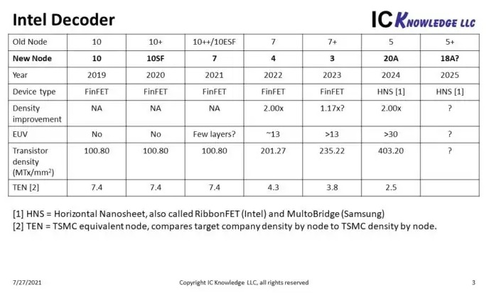
Figure 1 presents a chart comparing the Intel previous and current node names and process features. Please note that density improvement and transistor density numbers include IC Knowledge projections.

Figure 1. Intel Decoder
Comparisons
To put all of this in perspective I have produced trend plots versus year for density and performance. To make this a consistent comparison I have used full production dates for all three companies.
Figure 2 presents transistor per millimeter squared for Intel, Samsung, and TSMC. We see Intel passing Samsung in 2023 but still slightly lagging TSMC in 2025. Once again these density numbers include IC Knowledge projections.

Figure 2. Transistor Density Trend.
Figure 3 presents relative performance trends for Intel, Samsung, and TSMC. We believe Intel already leads Samsung, but will still slightly lag TSMC in 2025.

Figure 3. Performance Trend.
Conclusion
Intel Accelerated is an impressive presentation and set of technical goals. If Intel executes on this roadmap, they should achieve the process performance they need to field competitive microprocessors. However, we do still expect TSMC to maintain a lead through 2025.
Also Read:
VLSI Technology Symposium – Imec Alternate 3D NAND Word Line Materials
VLSI Technology Symposium – Imec Forksheet
VLSI Symposium – TSMC and Imec on Advanced Process and Devices Technology Toward 2nm
Share this post via:


Comments
15 Replies to “Intel Accelerated”
You must register or log in to view/post comments.