You are currently viewing SemiWiki as a guest which gives you limited access to the site. To view blog comments and experience other SemiWiki features you must be a registered member. Registration is fast, simple, and absolutely free so please,
join our community today!
One of the first blogs I wrote on SemiWiki was on clock domain crossing (CDC). I thought it was rather a specialized subject, a sort of minority interest. It turned out to be one of the most-read blogs I’ve written. Modern SoCs have lots of unrelated clocks, maybe hundreds, and so ensuring that signals going from one clock domain… Read More
In recent times semiconductor companies have revealed their intentions to license their in-house processor architectures for the first time – IBM want to license their Power CPU architecture, nVidia to license their GPU architecture. Most recently, a rumor has surfed: Qualcomm will license their DSP architecture. We should… Read More
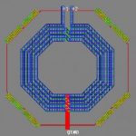
In many designs, an on chip inductor is created as though it were simply a device with an L and a Q value. Of course this view would seem to make life simpler for designers and the tools they use. But in reality even a simple inductor is really a complex compound structure with many electromagnetic elements interacting in complex ways.… Read More
ARM announced their quarterly results early this morning. ARM’s results are a funny mixture of backward looking information such as royalties which are reported a quarter late since they have to wait for their licensees to work out how many they shipped, and some very forward looking such as new licenses, which bring some… Read More
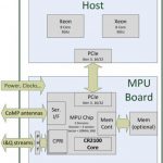
One thing that I learned about at the Liney Microprocessor Conference last week was C-RAN which stands for Cloud Radio Access Networks. The technology is created by ASOCS who are working with China Mobile as the driving customer. And before you dismiss that as just being one network interested in the technology, China Mobile has… Read More
The Biggest Private EDA Companyby admin on 10-21-2013 at 5:02 pmCategories: EDA
I talked this morning with fellow Brit David Halliday. More importantly, he is CEO of Silvaco, which he thinks must be the biggest private EDA company in the world. He didn’t reveal their revenue numbers but they have around 250-300 people and are profitable so you can make your own estimate.
David became CEO when Ivan Pesic,… Read More
I’m a big fan of lunch and learns, mainly because I’m a big fan of lunch but I also like to learn. I’m also a big fan of Tanner EDA which is why I helped organize this event. Face to face interaction amongst the fabless semiconductor ecosystem is critical to our success so stop on by and network, lunch is on me.
Take a look at the Brief History… Read More
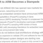
I have been at the Linley Microprocessor Conference today. This is the one that is not about mobile: about servers, networking, base-stations. Probably the most important story about the whole industry is that the “shift to ARM becomes a stampede.”
In this market it seems to be driven by the 64-bit ARMv8 instruction… Read More
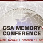
The GSA Memory+ conference Taiwan will take place on (Halloween!) October 31, 2013 at the Regent Taipei, Taiwan. The main theme of this year is highlighting Memory—the Critical Enabler for Prominent and Emerging Applications in System Logic Solutions.
GSA Memory+ Conference is the global industry event dedicated to all memory… Read More
The deadline for panel sessions, workshops, tutorials and co-located conferences for DAC 2014 is October 21st. That’s next Monday!
DAC 2014 will not only focus on EDA and embedded systems and software but
also include:
- design methods for automotive systems and software
- hardware and embedded systems security
- IP (semiconductor
…
Read More


Enhancing Multi-Domain System Simulation with FMI Co-Simulation