
A couple of weeks ago, Xilinx and TSMC announced the production release of the Virtex-7 HT family, the industry’s first heterogeneous 3D ICs in production. With this milestone, all Xilinx 28nm 3D IC families are now in volume production. These 28nm devices were developed on TSMC’s Chip-on-Wafer-on-Substrate (CoWoS) 3D IC process.
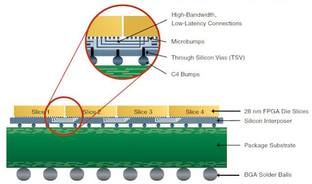
 A couple of years ago Xilinx announced what was then the first production part using a 2.5D silicon interposer. The part consisted of four rectangular die on a square silicon interposer. The die were regular FPGA die, flipped onto the interposer. The interposer had routing and through-silicon-vias (TSVs) to power up and connected the four die. It was a huge part. At a 3D symposium in 2011 eSilicon ran the publicly available information about this part through their cost model and reckoned yield would go from 25% for a huge square die to 75% with the smaller rectangular die. Even with the cost of the interposer eSilicon reckoned the cost saving to be around 50%. This was a very high end Xilinx part that apparently has a list price of tens of thousands of dollars, so even though it was in production, the volumes would have been very limited. Plus it was not a heterogeneous 3D design, all four slices were identical. I am sure Xilinx made this part not just because it was cost-effective but as a pipe-cleaner for interposer-based FPGAs and I’m sure they learned a lot.
The significance of 3D is two fold. Firstly, it allows Xilinx to manufacture FPGAs that are too big to do monolithically. Remember that as die size increases, you get fewer die per wafer but also the chance of an entire FPGA avoiding a critical defect decreases exponentially. You don’t avoid the first cost kicker by doing 3D, the die per wafer decreases whether you do multiple small die or one big one. Actually that is not quite true, there are probably some improvements around the edge of the wafer where a little less of the silicon out there is wasted. However, the second cost can be a big difference, with the smaller die yielding very much higher than the large one that might barely yield at all. For some applications, such as SoC prototyping, having a very big array is a big advantage over multiple smaller arrays since it avoids having to partition the SoC design and worry about the very different timing paths between arrays compared to on-array.
However the other significance is that by mixing die (and probably process) Xilinx can make parts like the Virtex-7 H580T which in addition to the array contains sixteen 28Gbps transceivers meaning that you can drive a 100Gbps optical module using only four transceivers compared to ten 10Gbps that you would need on a normal (not heterogeneous 3D) FPGA. That is what makes these parts the first heterogeneous 3D designs in volume production.
The Xilinx press release with more details is here.
More articles by Paul McLellan…


Comments
There are no comments yet.
You must register or log in to view/post comments.