You are currently viewing SemiWiki as a guest which gives you limited access to the site. To view blog comments and experience other SemiWiki features you must be a registered member. Registration is fast, simple, and absolutely free so please,
join our community today!
I just did a Google search for “3D IC”, and was stunned to see it return a whopping 476,000 results. This topic is trending, because more companies are using advanced IC packaging to meet their requirements, and yet the engineers doing the 3D IC design have new challenges to overcome. One of those challenges is creating… Read More
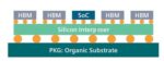
The move from single-chip design to system-in-package design has created many challenges. The rise of 2.5D and 3D technology has set the stage for this. Beyond the modeling requirements and the need for ecosystem collaboration to get those models, there is a significant challenge in understanding the data. The only way to truly… Read More
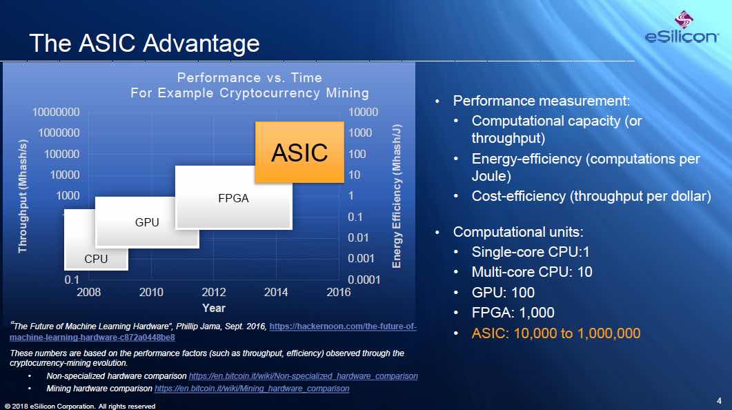
The progression from CPU to GPU, FPGA and then ASIC affords an increase in throughput and performance, but comes at the price of decreasing flexibility and generality. Like most new areas of endeavor in computing, artificial intelligence (AI) began with implementations based on CPU’s and software. And, as have so many other applications,… Read More
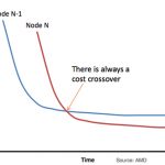
Following Moore’s Law down to 10 or even 7 nm labeled feature size demands US $ hundreds of millions of up-front investment, a very large design team and two or more years of development time. These parameters suggest that it only makes sense for very high volume applications to continue on the shrink path to increase SoCs’ functionalities.… Read More
More news from the 3DASIP conference. Chet Palesko of SavanSys Solution had an interesting presentation with the same title as this blog (although this blog draws from several other presentations too). Chet took a look at what aspects of 3D are likely to get cheaper going forward. He took as a starting point that stuff that is not … Read More
3DIC in Burlingameby Paul McLellan on 12-01-2014 at 7:00 amCategories: Events
Every year in December is what I think of as the main 3D IC conference where you can get up to speed on all the latest. Officially it is called 3D Architectures for Semiconductor and Packaging or 3D ASIP. It is held in the Hyatt Regency in Burlingame (the one right by 101 near the airport). This year it is from December 10-12th.
The first… Read More
At the GSA Silicon Summit this afternoon there was a discussion of 3D IC and 2.5D IC. The session was moderated by Javier DeLaCruz of eSilicon and the panelists were:
- Calvin Cheung of ASE (an OSAT)
- Gil Lvey of OptimalTest (a test house)
- Bob Patti of Tezzaron (semiconductor company specializing in TSV-based designs)
- Riko Radojcic
…
Read More
Every year the GSA holds the GSA Silicon Summit. This year it is on April 10th at the Computer History Museum. It runs from 9am until 2.15pm. This year the focus is mostly on technologies other than simply scaling semiconductor technology. The meeting is divided into 3 sessions, each of which starts with a presentation and then is … Read More
The first keynote at the Burlingame 3D conference was by Doug Yu of TSMC. Not surprisingly he was talking about 3D. In particular, TSMC has WLSI technology that they call CoWoS, which stands for chip-on-wafer-on-substrate which pretty much describes how it is built. This is the technology that Xilinx uses for its recently announced… Read More
AMD Goes 3Dby Paul McLellan on 12-13-2013 at 7:16 pmCategories: EDA
I attended the 3D packaging conference in Burlingame this week. The most interesting presentation to me was by Bryan Black of AMD. He argued very convincingly that Moore’s Law is basically over for the PC microprocessor business and the way forward is going to be 3D. AMD are clearly working on all this.
Increased density and… Read More