You are currently viewing SemiWiki as a guest which gives you limited access to the site. To view blog comments and experience other SemiWiki features you must be a registered member. Registration is fast, simple, and absolutely free so please,
join our community today!
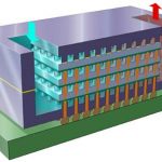
A couple of weeks ago, Xilinx and TSMC announced the production release of the Virtex-7 HT family, the industry’s first heterogeneous 3D ICs in production. With this milestone, all Xilinx 28nm 3D IC families are now in volume production. These 28nm devices were developed on TSMC’s Chip-on-Wafer-on-Substrate (CoWoS)… Read More
GlobalFoundries had several interesting things at the ARM TechCon last week. Firstly, GlobalFoundries won the best in show award in the chip design category recognizing the best-in-class technologies introduced since the last TechCon.
Earlier in the summer GlobalFoundries and ARM announced the ARM Cortex-A12 processor,… Read More
For the tenth year, the big 3DIC conference takes place in the Hyatt Regency at Burlingame (just south of San Francisco Airport). Officially it is 3D Architectures for Semiconductor Integration and Packaging or ASIP. This year there have already been some significant 3D announcements: TSMC’s 3D program, and Micron’s… Read More
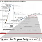
With the uncertainties around timing of 450mm wafers, EUV (whether it works at all and when) and new transistor architectures it is unclear whether Moore’s law as we know it is going to continue, and in particular whether the cost per transistor is going to remain economically attractive especially for consumer markets … Read More
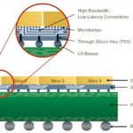
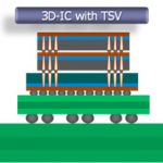
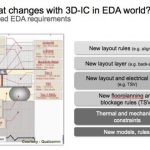
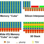
A couple of weeks ago was the 3D Architectures for Semiconductor Integration and Packagingconference in Redwood City. Cadence presented the changes that they have been making to their tool flow to enabled 2.5D (interposer-based) and true 3D TSV-based designs. You know what TSV stands for by now right? Through-silicon-via, … Read More
There is obviously a lot going on in 3D IC these days. And I don’t mean at the micro level of FinFETs which is also a way of going vertical. I mean through-silicon-via (TSV) based approaches for either stacking die or putting them on an interposer. Increasingly the question is no longer if this technology will be viable (there… Read More
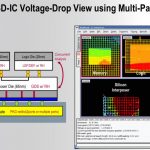
For many, maybe most, big designs, Apache’s RedHawk is the signoff tool for analyzing issues around power: electromigration, power supply droop, noise, transients and so on. But the latest designs have some issues: they are enormous (so you can’t just analyze them naively any more than you can run a Spice simulation… Read More
EDPS: 3D ICs, part IIby Paul McLellan on 04-12-2012 at 10:00 pmCategories: EDA, Events
Part I is here.
In the panel session at EDPS on 3D IC a number of major issues got highlighted (highlit?).
The first is the problem of known-good-die (KDG) which is what killed off the promising multi-chip-module approach, perhaps the earliest type of interposer. The KDG problem is that with a single die in a package it doesn’t… Read More
EDPS: 3D ICs, part Iby Paul McLellan on 04-10-2012 at 10:00 pmCategories: EDA, Events
The second day (more like a half-day) of EDPS was devoted to 3D ICs. There was a lot of information, too much to summarize in a few hundred words. The keynote was by Riko Radojcic of Qualcomm, who has been a sort of one-man-band attempting to drive the EDA and manufacturing industries towards 3D. Of course it helps if you don’t … Read More
And no red and green glasses required.
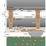
I remember the first time I heard about a Through Silicon Via (TSV), punching a hole through the entire wafer to make an electrical connection at the back, like we do all the time in printed circuit boards with through plated holes. I thought someone was trying one on and trying to make me look a fool.… Read More