

 Part I is here.
In the panel session at EDPS on 3D IC a number of major issues got highlighted (highlit?).
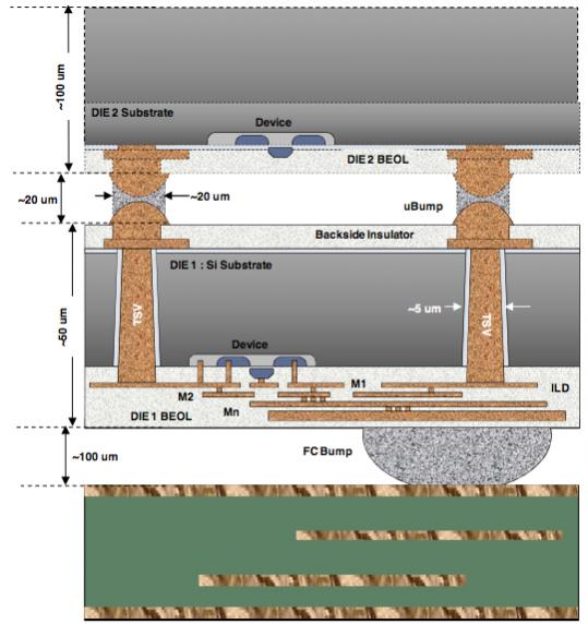
The first is the problem of known-good-die (KDG) which is what killed off the promising multi-chip-module approach, perhaps the earliest type of interposer. The KDG problem is that with a single die in a package it doesn’t make too much sense to invest a lot of money at wafer sort. If the process is yielding well, then identify the bad die cheaply and package up the rest. Some will fail final test due to bonding and other packaging issues, and some die weren’t good to begin with (so you are chucking out a bad die after having spent a bit too much on it). With a stack just 4 die and a wafer sort that is 99% effective (only 1% of bad die get through), the stack only yields 95% and those 5% discarded do not just contain bad die, there are (almost) 3 good die and an expensive package too. Since these die are not going to be bonded out, they don’t automatically have bond pads for wafer sort to contact and it is beyond the state of the art to put a probe on a microbump (and at 1gm of force on 20um bump, that is enormous pressure) so preparing for wafer sort requires some thought.
The next big problem is who takes responsibility for what, in particular, when a part fails who is responsible. Everyone is terrified of the lawyers. The manufacturing might be bad, the wafer test may be inadequate, the microbumping assembly may be bad, the package may be bad and, generally, assigning responsibility is harder. It looks likely that there will end up being two manufacturers responsible, the foundry who does the semiconductor manufacturing, the TSV manufacturing and (maybe) the microbumps. And the assembly house or OSAT as we are now meant to call them (outsourced semiconductor assembly and test) who puts it all together and does final test.
The third big problem is thermal analysis. Not just the usual how hot does the chip get and how does that affect performance. But there are different thermal coefficients of expansion which can cause all sorts of mechanical failure of the connections in the stack. This was one of the biggest challenges in getting surface mount technology for PCBs to work reliably: the parts kept falling off the board due to the different reaction to thermal stresses. Not good if it was in your plane or car.
 Philip Marcoux had a quote from the days of surface mount: “successful design and assembly of complex fine-pitch circuit boards is a team sport.” And 3D chips obviously are too. The team is at least:
- the device suppliers (maybe more than one for different die, maybe not)
- the interposer designer and supplier (if there is one)
- the assembler
- the material suppliers (different interconnects, different TSVs, different device thicknesses will need different materials, solder, epoxy…)
- an understanding pharmacist or beverage supplier (to alleviate stresses)
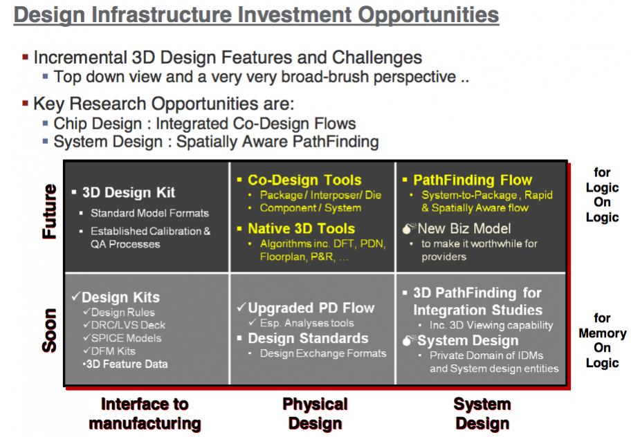
His prescription for EDA:
- develop a better understanding of the different types of TSV (W vs Cu; first/middle/last etc)
- coordinate with assembly equipment suppliers to create an acceptable file exchange for device registration and placement
- create databases of design guidelines to help define the selection of assembly processes, equipment and materials
- encourage and participate in the creation of standards
- develop suitable floorplanning tools for individual die
- develop 3D chip-to-chip planning tools
- provide thermal planning tools (chips in the middle get hot)
- provide cost modeling tools to address designer driven issues such as when to use 3D vs 2.5D interposer vs big chip
It is unclear to me whether these are all really the domain of EDA. Process cost modeling is its own domain and not one where EDA is well-connected. Individual semiconductor companies and assembly houses guard their cost models as tightly as their design data.
Plus one of the challenges with standards is when to develop them. Successful standards require that you already know how to do whatever is being standardized and as a result most successful standards start life as a de facto standard and then the known rough edges are filed off.
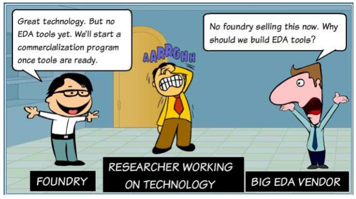 As always with EDA, one issue is how much money is to be made. EDA tools partially make money based on how valuable they are, but also largely by how many licenses large semiconductor companies need. In practice, the tools that make money either run for a long time (STA, P&R, DRC) or you sit in front of them all day (layout, some verification). Other tools (high level synthesis, bus register automation, floorplanning) suffer from what I call the “Intel only needs one copy” problem, that they don’t stimulate license demand in a natural way (although rarely in such an extreme way that Intel really only needs a single copy, of course).


Consolidation and Competition: Who is Winning the $4.5 Billion Interface IP Race?