
And no red and green glasses required.
I remember the first time I heard about a Through Silicon Via (TSV), punching a hole through the entire wafer to make an electrical connection at the back, like we do all the time in printed circuit boards with through plated holes. I thought someone was trying one on and trying to make me look a fool. But it is real and becoming realer (as my daughter used to say).
3D integrated circuits, stacking lots of die on top of each other, is a bit like boiling the ocean. Everything has to change at once. There is little point in being able to circuit simulate a TSV without being able to handle it in place and route.
Today, Synopsys announced that they were at least heating up the ocean. Their solution involves tools from TCAD to test, from floor-planning (how many floors?) to physical layout.
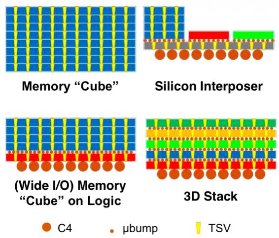
In my opinion (which is obviously spot-on) nobody is interested in 3D IC yet. By which I mean punching TSVs through active area and building true stacks of die. The one exception is putting stacks of memory on top of processors and lots of progress has been made here in defining the wide I/O standard whereby you can (or at least should be able) to use any memory vendor you want and switch between them.
The baby-steps version of 3D is 2½D, namely putting die on a silicon interposer. The big advantage is that the die and their designers don’t need to know a lot about TSVs since there are none in their designs. They exist only on the interposer. There are two big problems with punching TSVs all over a die. One is that they have a huge exclusion area known as a Keep Out Zone (KOZ) and a large part of the reason is that the process of making the TSV stresses the silicon (it uses plasma) leading to threshold shifts in nearby transistors. These are fairly predictable so in the best of all worlds these shifts could be used to advantage, but for sure they complicate doing static timing analysis beyond where anyone wants to go yet.
Synopsys has been coordinating an effort across their whole tool chain to get 3D ready (as, to be fair, has Cadence and Mentor in the stuff they do). From TCAD tools about how to analyze a TSV, up to higher level stuff like place and route. One area of particular intensity is extraction and analysis: the size of a design can suddenly be many die, and the analysis involve die, bumps, little bonds, interposers, C5 bonds, package pins and even the circuit board. That can be a lot of data.
One area where there is a problem is thermal. The people who do really accurate thermal analysis can’t cope with the billions of devices on a die-stack. The people who analyze die don’t have the accuracy to cope with multiple die, in multiple technologies, separated by thermally conductive air and micro-balls etc. But this is clearly something where good information is needed. At one level, multi-die stack can be good (every die has another die as a heatsink) but eventually all that heat needs to get out. Synopsys admit that this is a problem they don’t yet address and don’t really have a good answer too even with their partners.
Another major challenge is test. We never used to worry that much about wafer test, weed out the obviously bad die, package up the rest and throw a few away. When you start to package up multiple die in a package, knowing if a die is good becomes really important. If you are wrong, you don’t just throw away a die that was already bad having spent a bit too much on it, you throw away a set of other good die. So wafer sort, the neglected sibling of test, will become really important. You need lots of known-good die.
Although Synopsys’s announcement is all about 3D it is really about 2½ because that’s where the real market is today. We will get to 3D (especially if EUV doesn’t work out so we have to go vertical rather than horizontal) but not for a bit yet.
I can’t make it to SNUG but there are several presentations about 3D there. One from Xilinx, a pioneer in the space, who are shipping a high end FPGA on a silicon interposer, about how they did it. Independent estimates from eSilicon (and to be fair they didn’t have access to Xilinx raw data) reckons they are laughing all the way to the bank compared to trying to build a huge die and get it to yield, an eye-opener to me when I saw the analysis last year at a 3D symposium. 3D is expensive, but big die can be even worse.


Comments
There are no comments yet.
You must register or log in to view/post comments.