You are currently viewing SemiWiki as a guest which gives you limited access to the site. To view blog comments and experience other SemiWiki features you must be a registered member. Registration is fast, simple, and absolutely free so please,
join our community today!
EDPS Montereyby Paul McLellan on 03-17-2012 at 8:00 amCategories: EDA, Events
Every year in Monterey is a relatively small conference that looks at the design process, EDPS, the electronic design process symposium. I gave a keynote there a couple of years ago, but you don’t have to listen to me this time. The keynotes are from:
- 1st day: Misha Buric, CTO of Altera, talking about SoC FPGAs and other things
…
Read More
When process nodes reached 28 nm and below, it appeared that design density is reaching a saturation point, hitting the limits of Moore’s law. I was of the opinion that the future of microelectronic physical design was limited to 20 and 14 nm being addressed by technological advances such as FinFETs, double patterning, HKMG (High-k… Read More
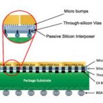
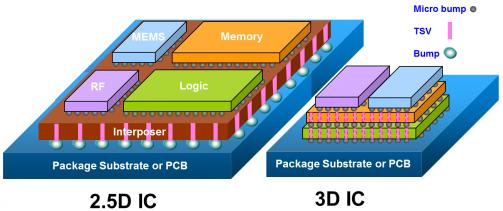
The ASIC business is getting more and more complicated. The ability to produce innovative die at a competitive price to solve increasingly complex problems just isn’t enough. The technology required to package that die is now front and center.
Here, at the junction of advanced design, process technology and state-of-the art … Read More