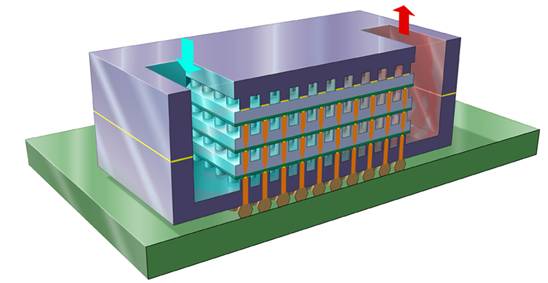


 There is obviously a lot going on in 3D IC these days. And I don’t mean at the micro level of FinFETs which is also a way of going vertical. I mean through-silicon-via (TSV) based approaches for either stacking die or putting them on an interposer. Increasingly the question is no longer if this technology will be viable (there are already production designs) but when it will go mainstream.
The most informative conference I’ve attended on this is held in December. This year it is in Sofitel in Redwood City (down near the Oracle towers) from December 12-14th at the end of this week. If you are interested in this area at all then you should be attending. I was planning on attending myself (they gave me a press pass) but I’m actually going to be out of town.
This meeting is not focused on EDA, although it does cover that. It covers the entire ecosystem and all sorts of issues around who does what on the supply chain, how you keep wafers from breaking once you’ve thinned them (glue them onto something else) and so on. It gives the best overview of all the issues of anything I’ve been to.
I won’t try and summarize the whole agenda, you can look at it for yourself here (pdf). But the first morning is all keynotes, all the time, from 8-10.30:
- The Evolution of 3-D ICs: Leaping Ahead of Moore’s Law to Deliver a 6.8B Transistor Device , Liam Madden, Xilinx
- Revolutionary Changes in Memory Technology and the Role of 3-D, Thomas Pawlowski, Micron
- Moore’s Law, Semiconductor Economics, and Other Bellwethers of 3-D IC, Vinod Kariat, Cadence
- Technical Challenges and Progress in an Open Supply Chain Model, David McCann, Global Foundries
Online registration still seems to be open here.


Podcast EP357: How Gonka is Changing the Way AI is Accessed with David Liberman