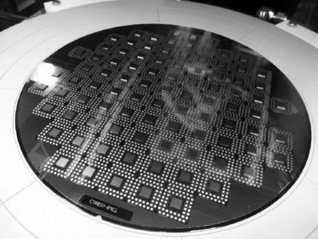

 The first keynote at the Burlingame 3D conference was by Doug Yu of TSMC. Not surprisingly he was talking about 3D. In particular, TSMC has WLSI technology that they call CoWoS, which stands for chip-on-wafer-on-substrate which pretty much describes how it is built. This is the technology that Xilinx uses for its recently announced high end arrays which I already wrote about here.
The basic driver, in Doug’s view, is that on-chip interconnect is not scaling with Moore’s Law and so alternative approaches are required. He didn’t talk about cost (the manufacturers rarely do but when they talk about higher performance and lower power and don’t mention cost then you have to know the news is not wonderful. At best 20nm is flat to 28nm cost wise).
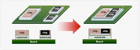
Another issue is that at 16nm FinFET it is not clear that everything we used to be able to integrate onto a chip, such as RF and analog, will still work. At least at acceptable cost. One obvious advantage of any sort of 3D chip is the ability to mix die from different processes, such as having a 28nm didital chip with 90nm RF/analog (what Doug calls “a ranch in the middle of Manhattan”) and move the 10um inductor off-chip. This saves chip area, cost and power.
TSMC is looking at how to ramp this 3D technology fast to volume. The costs of CoWoS are still too high but there is not really any substitute for the type of yield learning that comes from building products at volume. TSMC sees their goal to grow from a chip foundry to a subsystem foundry, delivering integrated subsystems consisting of die from multiple processes integrated together using CoWoS. He thinks that there are at most 5 companies that could potentially be suppliers into this market.
During questions he was asked about TSMC’s views on TSV holes. There are a number of ways of building TSVs. Via first means that the TSVs are created before the first layer of metal (I don’t think it is possible to do them before the transistors due to the high temperatures used in the FEOL, but I am certainly not a process expert). Via middle means that some metal is created and then the TSV is added and additional metal layers later to hook everything up. It is also possible to create the via from the backside of the wafer. The TSMC view is to do the TSVs as early as possible. Someone pointed out that you cannot use copper for the TSV if you do via first but Doug said that was not true and TSMC uses it today.
Eventually TSMC will scale all this to 450mm but it is too hard to move to 450mm at the same time as a node-change, so that 450mm will first be introduced on a node that is already running at volume. 28nm is my guess. But for wafer scale integration like CoWoS then 450mm is ideal since the costs are lower and they are not trying to get critical features to yield right out at the edge of the wafer where everything is more difficult.
 The general impression from the keynotes at 3D ASIP was that:
- 3D (which really means 2.5D and memory stacks for now) is real and 2014 will start to ramp
- costs will come down with yield learning once a few million units have been built and shipped
- driver will be high end initially (HPC, networking) not mobile, but mobile is the dream to really drive volume
- the biggest problem is, surprisingly, not the TSVs but bond of the wafer onto a substrate for thinning, and then debonding the thin wafer afterwards and all the handling
- interposers will have more than wires on. Once costs come down it makes no sense to leave the I/Os on a 20nm die instead of putting them on the interposers (they don’t really shrink anyway). Also power transistors, capacitors etc. If only wires, organic substrates will probably win.
- component cost of a 3D chip will not be less than multiple components but the saving at the system level might be very large
More articles by Paul McLellan…


Comments
0 Replies to “TSMC: 3D, 450mm, CoWoS and More”
You must register or log in to view/post comments.