You are currently viewing SemiWiki as a guest which gives you limited access to the site. To view blog comments and experience other SemiWiki features you must be a registered member. Registration is fast, simple, and absolutely free so please,
join our community today!
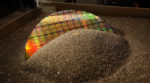
Pinpointing exactly when 450mm died is tricky. Intel’s pullback in 2014 has been cited as a pivotal moment because it was the main backer of the proposed transition, as it had been for the shift to 150mm (6-inch) wafers in the early 1980s.
However, the participation of global foundry leader TSMC was also seen as crucial if 450mm wafers… Read More
I spent several days this week at the SEMI International Strategy Symposium (ISS). One of the talks was “Can the Semiconductor Industry Reach $1T by 2030” given by Bob Johnson of Gartner. His conclusion was, that $1 trillion dollars is an aggressive forecast for 2030 but certainly we should reach $1 trillion dollars in the next 10… Read More
The worldwide revenue of semiconductor industry has remained flat in last few years; to be more precise, overall semiconductor revenue declined by 1.9% in 2015 and Gartner forecasts it to further decline by 0.6% in 2016. The total revenue was at record high of $340.3 billion in 2014.
Well, semiconductor industry has matured. A … Read More
Let’s start with yesterday evening, so technically yesterday. It was July 14th, which is the equivalent of Independence Day in France. So the perfect day for Leti, based in Grenoble, to present a lot of the work that they are doing on 3D “more than Moore” type technologies, including photonics. Also, wafer-scale… Read More
Founded in 1971 (2015: 45th year), SEMICON West 2015 is coming to the Moscone Center in San Francisco on from Tuesday, July 14[SUP]th[/SUP] to Thursday, July 16[SUP]th[/SUP]. SEMICON is the premier show for equipment and materials companies supporting the semiconductor, MEMS and solar industries.
The main ways to get value … Read More
I spent all of last week at SEMICON West meeting with customers, potential customers, partners and various industry analysts and experts. I was involved in many interesting discussions over the course of the week and I thought I would share some of the more interesting observations:
Alternate Fin Materials Pushed Out
I have for… Read More
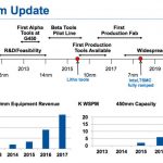
Paul Farrar, the General Manager of the Global 450mm Consortium (G450C) presented at the SEMI ISS conference today. What is G450C, it is a public-private consortium to develop a cost-effective 450mm wafer fabrication infrastructure, develop equipment prototypes and coordinate the industry move to 450mm. It is located in Albany… Read More
Technology Challenges: Intel, IBM, Xilinx, GlobalFoundries, IMECby Paul McLellan on 01-14-2014 at 7:00 pmCategories: ESD Alliance, FPGA, GlobalFoundries, Intel Foundry, Semiconductor, Semiconductor Services, Xilinx
I spent the day at the SEMI Industry Strategy Symposium in Half Moon Bay. The early part of the day was devoted to technology challenges. Obviously everyone did not say exactly the same things, and had a little bit of a different spin depending on what business they are in. But there was a lot of commonality between Intel, IBM, Xilinx… Read More
The first keynote at the Burlingame 3D conference was by Doug Yu of TSMC. Not surprisingly he was talking about 3D. In particular, TSMC has WLSI technology that they call CoWoS, which stands for chip-on-wafer-on-substrate which pretty much describes how it is built. This is the technology that Xilinx uses for its recently announced… Read More
I attended the semi-annual SEMI Silicon Valley Lunch meeting last week. The semiconductor equipment people are the ones that really know what is going on. People can talk about capex numbers on conference calls but it is the equipment vendors who either do or do not get orders for particular types of equipment. In turn, the analysts… Read More