Threads
XF\Mvc\Entity\ArrayCollection Object
(
[entities:protected] => Array
(
[25572] => ThemeHouse\XPress\XF\Entity\Thread Object
(
[_uniqueEntityId:XF\Mvc\Entity\Entity:private] => 57
[rootClass:protected] => XF\Entity\Thread
[_useReplaceInto:protected] =>
[_newValues:protected] => Array
(
)
[_values:protected] => Array
(
[thread_id] => 25572
[node_id] => 2
[title] => Is SK Hynix Buying Intel’s Ohio Fab? Korean Chipmaker Denies Report — Now All Eyes Are on Earnings
[reply_count] => 53
[view_count] => 4228
[user_id] => 5
[username] => Daniel Nenni
[post_date] => 1784736405
[sticky] => 0
[discussion_state] => visible
[discussion_open] => 1
[discussion_type] => discussion
[first_post_id] => 101991
[first_post_reaction_score] => 0
[first_post_reactions] => []
[last_post_date] => 1785302031
[last_post_id] => 102221
[last_post_user_id] => 14042
[last_post_username] => hist78
[prefix_id] => 0
[tags] => []
[custom_fields] => []
[vote_score] => 0
[vote_count] => 0
[featured] => 0
[type_data] => []
[index_state] => default
)
[_relations:protected] => Array
(
[User] => ThemeHouse\XLink\XF\Entity\User Object
(
[_uniqueEntityId:XF\Mvc\Entity\Entity:private] => 54
[rootClass:protected] => XF\Entity\User
[_useReplaceInto:protected] =>
[_newValues:protected] => Array
(
)
[_values:protected] => Array
(
[user_id] => 5
[username] => Daniel Nenni
[username_date] => 0
[username_date_visible] => 0
[email] => dnenni@semiwiki.com
[custom_title] => Founder
[language_id] => 1
[style_id] => 0
[style_variation] =>
[timezone] => America/Los_Angeles
[visible] => 1
[activity_visible] => 1
[user_group_id] => 3
[secondary_group_ids] => 4,5,132
[display_style_group_id] => 3
[permission_combination_id] => 88
[message_count] => 15875
[question_solution_count] => 0
[conversations_unread] => 0
[register_date] => 1280720820
[last_activity] => 1785296432
[last_summary_email_date] => 1605968657
[trophy_points] => 113
[alerts_unviewed] => 91
[alerts_unread] => 91
[avatar_date] => 1663211649
[avatar_width] => 110
[avatar_height] => 107
[avatar_highdpi] => 0
[avatar_optimized] => 0
[gravatar] =>
[user_state] => valid
[security_lock] =>
[is_moderator] => 1
[is_admin] => 1
[is_banned] => 0
[reaction_score] => 9726
[warning_points] => 0
[is_staff] => 1
[secret_key] => 0HwyUVVHCwJotUUVEpvqAclfYJdGNPpw
[privacy_policy_accepted] => 0
[terms_accepted] => 0
[vote_score] => 0
)
[_relations:protected] => Array
(
)
[_previousValues:protected] => Array
(
)
[_options:protected] => Array
(
)
[_deleted:protected] =>
[_readOnly:protected] =>
[_writePending:protected] =>
[_writeRunning:protected] =>
[_errors:protected] => Array
(
)
[_whenSaveable:protected] => Array
(
)
[_cascadeSave:protected] => Array
(
)
[_behaviors:protected] =>
)
[Forum] => XF\Entity\Forum Object
(
[_uniqueEntityId:XF\Mvc\Entity\Entity:private] => 56
[rootClass:protected] => XF\Entity\Forum
[_useReplaceInto:protected] =>
[_newValues:protected] => Array
(
)
[_values:protected] => Array
(
[node_id] => 2
[discussion_count] => 8912
[message_count] => 65111
[last_post_id] => 102221
[last_post_date] => 1785302031
[last_post_user_id] => 14042
[last_post_username] => hist78
[last_thread_id] => 25572
[last_thread_title] => Is SK Hynix Buying Intel’s Ohio Fab? Korean Chipmaker Denies Report — Now All Eyes Are on Earnings
[last_thread_prefix_id] => 0
[moderate_threads] => 0
[moderate_replies] => 0
[allow_posting] => 1
[count_messages] => 1
[auto_feature] => 0
[find_new] => 1
[allow_index] => allow
[index_criteria] =>
[field_cache] => []
[prefix_cache] => []
[prompt_cache] => []
[default_prefix_id] => 0
[default_sort_order] => last_post_date
[default_sort_direction] => desc
[list_date_limit_days] => 0
[require_prefix] => 0
[allowed_watch_notifications] => all
[min_tags] => 0
[forum_type_id] => discussion
[type_config] => {"allowed_thread_types":["poll"]}
)
[_relations:protected] => Array
(
[Node] => XF\Entity\Node Object
(
[_uniqueEntityId:XF\Mvc\Entity\Entity:private] => 55
[rootClass:protected] => XF\Entity\Node
[_useReplaceInto:protected] =>
[_newValues:protected] => Array
(
)
[_values:protected] => Array
(
[node_id] => 2
[title] => SemiWiki Main Forum ( Ask the Experts! )
[description] => Post your questions to the experts here!
[node_name] =>
[node_type_id] => Forum
[parent_node_id] => 1
[display_order] => 1
[display_in_list] => 1
[lft] => 2
[rgt] => 3
[depth] => 1
[style_id] => 0
[effective_style_id] => 0
[breadcrumb_data] => {"1":{"node_id":1,"title":"Main Category","depth":0,"lft":1,"node_name":null,"node_type_id":"Category","display_in_list":true}}
[navigation_id] =>
[effective_navigation_id] =>
)
[_relations:protected] => Array
(
)
[_previousValues:protected] => Array
(
)
[_options:protected] => Array
(
)
[_deleted:protected] =>
[_readOnly:protected] =>
[_writePending:protected] =>
[_writeRunning:protected] =>
[_errors:protected] => Array
(
)
[_whenSaveable:protected] => Array
(
)
[_cascadeSave:protected] => Array
(
)
[_behaviors:protected] =>
)
)
[_previousValues:protected] => Array
(
)
[_options:protected] => Array
(
)
[_deleted:protected] =>
[_readOnly:protected] =>
[_writePending:protected] =>
[_writeRunning:protected] =>
[_errors:protected] => Array
(
)
[_whenSaveable:protected] => Array
(
)
[_cascadeSave:protected] => Array
(
)
[_behaviors:protected] =>
)
[25610] => ThemeHouse\XPress\XF\Entity\Thread Object
(
[_uniqueEntityId:XF\Mvc\Entity\Entity:private] => 61
[rootClass:protected] => XF\Entity\Thread
[_useReplaceInto:protected] =>
[_newValues:protected] => Array
(
)
[_values:protected] => Array
(
[thread_id] => 25610
[node_id] => 2
[title] => China Begins Limited Production of Domestic Immersion DUV Machines
[reply_count] => 8
[view_count] => 1021
[user_id] => 29441
[username] => tonyget
[post_date] => 1785181506
[sticky] => 0
[discussion_state] => visible
[discussion_open] => 1
[discussion_type] => discussion
[first_post_id] => 102178
[first_post_reaction_score] => 2
[first_post_reactions] => {"1":2}
[last_post_date] => 1785295317
[last_post_id] => 102217
[last_post_user_id] => 20231
[last_post_username] => Barnsley
[prefix_id] => 0
[tags] => []
[custom_fields] => []
[vote_score] => 0
[vote_count] => 0
[featured] => 0
[type_data] => []
[index_state] => default
)
[_relations:protected] => Array
(
[User] => ThemeHouse\XLink\XF\Entity\User Object
(
[_uniqueEntityId:XF\Mvc\Entity\Entity:private] => 58
[rootClass:protected] => XF\Entity\User
[_useReplaceInto:protected] =>
[_newValues:protected] => Array
(
)
[_values:protected] => Array
(
[user_id] => 29441
[username] => tonyget
[username_date] => 0
[username_date_visible] => 0
[email] => tonygect@gmail.com
[custom_title] =>
[language_id] => 1
[style_id] => 0
[style_variation] =>
[timezone] => America/Los_Angeles
[visible] => 1
[activity_visible] => 1
[user_group_id] => 2
[secondary_group_ids] =>
[display_style_group_id] => 2
[permission_combination_id] => 8
[message_count] => 540
[question_solution_count] => 0
[conversations_unread] => 0
[register_date] => 1530379703
[last_activity] => 1785284607
[last_summary_email_date] =>
[trophy_points] => 63
[alerts_unviewed] => 0
[alerts_unread] => 0
[avatar_date] => 0
[avatar_width] => 0
[avatar_height] => 0
[avatar_highdpi] => 0
[avatar_optimized] => 0
[gravatar] =>
[user_state] => valid
[security_lock] =>
[is_moderator] => 0
[is_admin] => 0
[is_banned] => 0
[reaction_score] => 344
[warning_points] => 0
[is_staff] => 0
[secret_key] => p8Xu8RMcYNG2Mp-_wc8Za9aU-kUYGMwP
[privacy_policy_accepted] => 0
[terms_accepted] => 0
[vote_score] => 0
)
[_relations:protected] => Array
(
)
[_previousValues:protected] => Array
(
)
[_options:protected] => Array
(
)
[_deleted:protected] =>
[_readOnly:protected] =>
[_writePending:protected] =>
[_writeRunning:protected] =>
[_errors:protected] => Array
(
)
[_whenSaveable:protected] => Array
(
)
[_cascadeSave:protected] => Array
(
)
[_behaviors:protected] =>
)
[Forum] => XF\Entity\Forum Object
(
[_uniqueEntityId:XF\Mvc\Entity\Entity:private] => 56
[rootClass:protected] => XF\Entity\Forum
[_useReplaceInto:protected] =>
[_newValues:protected] => Array
(
)
[_values:protected] => Array
(
[node_id] => 2
[discussion_count] => 8912
[message_count] => 65111
[last_post_id] => 102221
[last_post_date] => 1785302031
[last_post_user_id] => 14042
[last_post_username] => hist78
[last_thread_id] => 25572
[last_thread_title] => Is SK Hynix Buying Intel’s Ohio Fab? Korean Chipmaker Denies Report — Now All Eyes Are on Earnings
[last_thread_prefix_id] => 0
[moderate_threads] => 0
[moderate_replies] => 0
[allow_posting] => 1
[count_messages] => 1
[auto_feature] => 0
[find_new] => 1
[allow_index] => allow
[index_criteria] =>
[field_cache] => []
[prefix_cache] => []
[prompt_cache] => []
[default_prefix_id] => 0
[default_sort_order] => last_post_date
[default_sort_direction] => desc
[list_date_limit_days] => 0
[require_prefix] => 0
[allowed_watch_notifications] => all
[min_tags] => 0
[forum_type_id] => discussion
[type_config] => {"allowed_thread_types":["poll"]}
)
[_relations:protected] => Array
(
[Node] => XF\Entity\Node Object
(
[_uniqueEntityId:XF\Mvc\Entity\Entity:private] => 55
[rootClass:protected] => XF\Entity\Node
[_useReplaceInto:protected] =>
[_newValues:protected] => Array
(
)
[_values:protected] => Array
(
[node_id] => 2
[title] => SemiWiki Main Forum ( Ask the Experts! )
[description] => Post your questions to the experts here!
[node_name] =>
[node_type_id] => Forum
[parent_node_id] => 1
[display_order] => 1
[display_in_list] => 1
[lft] => 2
[rgt] => 3
[depth] => 1
[style_id] => 0
[effective_style_id] => 0
[breadcrumb_data] => {"1":{"node_id":1,"title":"Main Category","depth":0,"lft":1,"node_name":null,"node_type_id":"Category","display_in_list":true}}
[navigation_id] =>
[effective_navigation_id] =>
)
[_relations:protected] => Array
(
)
[_previousValues:protected] => Array
(
)
[_options:protected] => Array
(
)
[_deleted:protected] =>
[_readOnly:protected] =>
[_writePending:protected] =>
[_writeRunning:protected] =>
[_errors:protected] => Array
(
)
[_whenSaveable:protected] => Array
(
)
[_cascadeSave:protected] => Array
(
)
[_behaviors:protected] =>
)
)
[_previousValues:protected] => Array
(
)
[_options:protected] => Array
(
)
[_deleted:protected] =>
[_readOnly:protected] =>
[_writePending:protected] =>
[_writeRunning:protected] =>
[_errors:protected] => Array
(
)
[_whenSaveable:protected] => Array
(
)
[_cascadeSave:protected] => Array
(
)
[_behaviors:protected] =>
)
)
[_previousValues:protected] => Array
(
)
[_options:protected] => Array
(
)
[_deleted:protected] =>
[_readOnly:protected] =>
[_writePending:protected] =>
[_writeRunning:protected] =>
[_errors:protected] => Array
(
)
[_whenSaveable:protected] => Array
(
)
[_cascadeSave:protected] => Array
(
)
[_behaviors:protected] =>
)
[25615] => ThemeHouse\XPress\XF\Entity\Thread Object
(
[_uniqueEntityId:XF\Mvc\Entity\Entity:private] => 65
[rootClass:protected] => XF\Entity\Thread
[_useReplaceInto:protected] =>
[_newValues:protected] => Array
(
)
[_values:protected] => Array
(
[thread_id] => 25615
[node_id] => 2
[title] => Taiwan detains Nvidia employee in Super Micro probe, Taiwan media says
[reply_count] => 3
[view_count] => 240
[user_id] => 36448
[username] => Paul2
[post_date] => 1785272884
[sticky] => 0
[discussion_state] => visible
[discussion_open] => 1
[discussion_type] => discussion
[first_post_id] => 102209
[first_post_reaction_score] => 2
[first_post_reactions] => {"1":2}
[last_post_date] => 1785286604
[last_post_id] => 102216
[last_post_user_id] => 20231
[last_post_username] => Barnsley
[prefix_id] => 0
[tags] => []
[custom_fields] => []
[vote_score] => 0
[vote_count] => 0
[featured] => 0
[type_data] => []
[index_state] => default
)
[_relations:protected] => Array
(
[User] => ThemeHouse\XLink\XF\Entity\User Object
(
[_uniqueEntityId:XF\Mvc\Entity\Entity:private] => 62
[rootClass:protected] => XF\Entity\User
[_useReplaceInto:protected] =>
[_newValues:protected] => Array
(
)
[_values:protected] => Array
(
[user_id] => 36448
[username] => Paul2
[username_date] => 0
[username_date_visible] => 0
[email] => pavel@noa-labs.com
[custom_title] =>
[language_id] => 1
[style_id] => 1
[style_variation] =>
[timezone] => Asia/Dubai
[visible] => 1
[activity_visible] => 1
[user_group_id] => 2
[secondary_group_ids] =>
[display_style_group_id] => 2
[permission_combination_id] => 8
[message_count] => 1430
[question_solution_count] => 0
[conversations_unread] => 0
[register_date] => 1606949753
[last_activity] => 1785289062
[last_summary_email_date] =>
[trophy_points] => 113
[alerts_unviewed] => 2
[alerts_unread] => 2
[avatar_date] => 0
[avatar_width] => 0
[avatar_height] => 0
[avatar_highdpi] => 0
[avatar_optimized] => 0
[gravatar] =>
[user_state] => valid
[security_lock] =>
[is_moderator] => 0
[is_admin] => 0
[is_banned] => 0
[reaction_score] => 838
[warning_points] => 0
[is_staff] => 0
[secret_key] => efEzRw1xb8upHCKpIENrLDbejN8APPhM
[privacy_policy_accepted] => 1606949753
[terms_accepted] => 1606949753
[vote_score] => 0
)
[_relations:protected] => Array
(
)
[_previousValues:protected] => Array
(
)
[_options:protected] => Array
(
)
[_deleted:protected] =>
[_readOnly:protected] =>
[_writePending:protected] =>
[_writeRunning:protected] =>
[_errors:protected] => Array
(
)
[_whenSaveable:protected] => Array
(
)
[_cascadeSave:protected] => Array
(
)
[_behaviors:protected] =>
)
[Forum] => XF\Entity\Forum Object
(
[_uniqueEntityId:XF\Mvc\Entity\Entity:private] => 56
[rootClass:protected] => XF\Entity\Forum
[_useReplaceInto:protected] =>
[_newValues:protected] => Array
(
)
[_values:protected] => Array
(
[node_id] => 2
[discussion_count] => 8912
[message_count] => 65111
[last_post_id] => 102221
[last_post_date] => 1785302031
[last_post_user_id] => 14042
[last_post_username] => hist78
[last_thread_id] => 25572
[last_thread_title] => Is SK Hynix Buying Intel’s Ohio Fab? Korean Chipmaker Denies Report — Now All Eyes Are on Earnings
[last_thread_prefix_id] => 0
[moderate_threads] => 0
[moderate_replies] => 0
[allow_posting] => 1
[count_messages] => 1
[auto_feature] => 0
[find_new] => 1
[allow_index] => allow
[index_criteria] =>
[field_cache] => []
[prefix_cache] => []
[prompt_cache] => []
[default_prefix_id] => 0
[default_sort_order] => last_post_date
[default_sort_direction] => desc
[list_date_limit_days] => 0
[require_prefix] => 0
[allowed_watch_notifications] => all
[min_tags] => 0
[forum_type_id] => discussion
[type_config] => {"allowed_thread_types":["poll"]}
)
[_relations:protected] => Array
(
[Node] => XF\Entity\Node Object
(
[_uniqueEntityId:XF\Mvc\Entity\Entity:private] => 55
[rootClass:protected] => XF\Entity\Node
[_useReplaceInto:protected] =>
[_newValues:protected] => Array
(
)
[_values:protected] => Array
(
[node_id] => 2
[title] => SemiWiki Main Forum ( Ask the Experts! )
[description] => Post your questions to the experts here!
[node_name] =>
[node_type_id] => Forum
[parent_node_id] => 1
[display_order] => 1
[display_in_list] => 1
[lft] => 2
[rgt] => 3
[depth] => 1
[style_id] => 0
[effective_style_id] => 0
[breadcrumb_data] => {"1":{"node_id":1,"title":"Main Category","depth":0,"lft":1,"node_name":null,"node_type_id":"Category","display_in_list":true}}
[navigation_id] =>
[effective_navigation_id] =>
)
[_relations:protected] => Array
(
)
[_previousValues:protected] => Array
(
)
[_options:protected] => Array
(
)
[_deleted:protected] =>
[_readOnly:protected] =>
[_writePending:protected] =>
[_writeRunning:protected] =>
[_errors:protected] => Array
(
)
[_whenSaveable:protected] => Array
(
)
[_cascadeSave:protected] => Array
(
)
[_behaviors:protected] =>
)
)
[_previousValues:protected] => Array
(
)
[_options:protected] => Array
(
)
[_deleted:protected] =>
[_readOnly:protected] =>
[_writePending:protected] =>
[_writeRunning:protected] =>
[_errors:protected] => Array
(
)
[_whenSaveable:protected] => Array
(
)
[_cascadeSave:protected] => Array
(
)
[_behaviors:protected] =>
)
)
[_previousValues:protected] => Array
(
)
[_options:protected] => Array
(
)
[_deleted:protected] =>
[_readOnly:protected] =>
[_writePending:protected] =>
[_writeRunning:protected] =>
[_errors:protected] => Array
(
)
[_whenSaveable:protected] => Array
(
)
[_cascadeSave:protected] => Array
(
)
[_behaviors:protected] =>
)
[25616] => ThemeHouse\XPress\XF\Entity\Thread Object
(
[_uniqueEntityId:XF\Mvc\Entity\Entity:private] => 69
[rootClass:protected] => XF\Entity\Thread
[_useReplaceInto:protected] =>
[_newValues:protected] => Array
(
)
[_values:protected] => Array
(
[thread_id] => 25616
[node_id] => 2
[title] => When Machines Speak, Matter Is Revealing Physics
Dr. Moh Kolbehdari
[reply_count] => 0
[view_count] => 93
[user_id] => 444140
[username] => moh.kolb
[post_date] => 1785276359
[sticky] => 0
[discussion_state] => visible
[discussion_open] => 1
[discussion_type] => discussion
[first_post_id] => 102214
[first_post_reaction_score] => 0
[first_post_reactions] => []
[last_post_date] => 1785276359
[last_post_id] => 102214
[last_post_user_id] => 444140
[last_post_username] => moh.kolb
[prefix_id] => 0
[tags] => []
[custom_fields] => []
[vote_score] => 0
[vote_count] => 0
[featured] => 0
[type_data] => []
[index_state] => default
)
[_relations:protected] => Array
(
[User] => ThemeHouse\XLink\XF\Entity\User Object
(
[_uniqueEntityId:XF\Mvc\Entity\Entity:private] => 66
[rootClass:protected] => XF\Entity\User
[_useReplaceInto:protected] =>
[_newValues:protected] => Array
(
)
[_values:protected] => Array
(
[user_id] => 444140
[username] => moh.kolb
[username_date] => 0
[username_date_visible] => 0
[email] => moh@kolbehdari.com
[custom_title] =>
[language_id] => 1
[style_id] => 0
[style_variation] =>
[timezone] => America/Phoenix
[visible] => 1
[activity_visible] => 1
[user_group_id] => 2
[secondary_group_ids] =>
[display_style_group_id] => 2
[permission_combination_id] => 8
[message_count] => 52
[question_solution_count] => 0
[conversations_unread] => 0
[register_date] => 1775069311
[last_activity] => 1785276417
[last_summary_email_date] => 1775069311
[trophy_points] => 8
[alerts_unviewed] => 1
[alerts_unread] => 1
[avatar_date] => 0
[avatar_width] => 0
[avatar_height] => 0
[avatar_highdpi] => 0
[avatar_optimized] => 0
[gravatar] =>
[user_state] => valid
[security_lock] =>
[is_moderator] => 0
[is_admin] => 0
[is_banned] => 0
[reaction_score] => 9
[warning_points] => 0
[is_staff] => 0
[secret_key] => EG539H6nqaiPLLZ4UXYEvAY-Py_6iJOA
[privacy_policy_accepted] => 1775069311
[terms_accepted] => 1775069311
[vote_score] => 0
)
[_relations:protected] => Array
(
)
[_previousValues:protected] => Array
(
)
[_options:protected] => Array
(
)
[_deleted:protected] =>
[_readOnly:protected] =>
[_writePending:protected] =>
[_writeRunning:protected] =>
[_errors:protected] => Array
(
)
[_whenSaveable:protected] => Array
(
)
[_cascadeSave:protected] => Array
(
)
[_behaviors:protected] =>
)
[Forum] => XF\Entity\Forum Object
(
[_uniqueEntityId:XF\Mvc\Entity\Entity:private] => 56
[rootClass:protected] => XF\Entity\Forum
[_useReplaceInto:protected] =>
[_newValues:protected] => Array
(
)
[_values:protected] => Array
(
[node_id] => 2
[discussion_count] => 8912
[message_count] => 65111
[last_post_id] => 102221
[last_post_date] => 1785302031
[last_post_user_id] => 14042
[last_post_username] => hist78
[last_thread_id] => 25572
[last_thread_title] => Is SK Hynix Buying Intel’s Ohio Fab? Korean Chipmaker Denies Report — Now All Eyes Are on Earnings
[last_thread_prefix_id] => 0
[moderate_threads] => 0
[moderate_replies] => 0
[allow_posting] => 1
[count_messages] => 1
[auto_feature] => 0
[find_new] => 1
[allow_index] => allow
[index_criteria] =>
[field_cache] => []
[prefix_cache] => []
[prompt_cache] => []
[default_prefix_id] => 0
[default_sort_order] => last_post_date
[default_sort_direction] => desc
[list_date_limit_days] => 0
[require_prefix] => 0
[allowed_watch_notifications] => all
[min_tags] => 0
[forum_type_id] => discussion
[type_config] => {"allowed_thread_types":["poll"]}
)
[_relations:protected] => Array
(
[Node] => XF\Entity\Node Object
(
[_uniqueEntityId:XF\Mvc\Entity\Entity:private] => 55
[rootClass:protected] => XF\Entity\Node
[_useReplaceInto:protected] =>
[_newValues:protected] => Array
(
)
[_values:protected] => Array
(
[node_id] => 2
[title] => SemiWiki Main Forum ( Ask the Experts! )
[description] => Post your questions to the experts here!
[node_name] =>
[node_type_id] => Forum
[parent_node_id] => 1
[display_order] => 1
[display_in_list] => 1
[lft] => 2
[rgt] => 3
[depth] => 1
[style_id] => 0
[effective_style_id] => 0
[breadcrumb_data] => {"1":{"node_id":1,"title":"Main Category","depth":0,"lft":1,"node_name":null,"node_type_id":"Category","display_in_list":true}}
[navigation_id] =>
[effective_navigation_id] =>
)
[_relations:protected] => Array
(
)
[_previousValues:protected] => Array
(
)
[_options:protected] => Array
(
)
[_deleted:protected] =>
[_readOnly:protected] =>
[_writePending:protected] =>
[_writeRunning:protected] =>
[_errors:protected] => Array
(
)
[_whenSaveable:protected] => Array
(
)
[_cascadeSave:protected] => Array
(
)
[_behaviors:protected] =>
)
)
[_previousValues:protected] => Array
(
)
[_options:protected] => Array
(
)
[_deleted:protected] =>
[_readOnly:protected] =>
[_writePending:protected] =>
[_writeRunning:protected] =>
[_errors:protected] => Array
(
)
[_whenSaveable:protected] => Array
(
)
[_cascadeSave:protected] => Array
(
)
[_behaviors:protected] =>
)
)
[_previousValues:protected] => Array
(
)
[_options:protected] => Array
(
)
[_deleted:protected] =>
[_readOnly:protected] =>
[_writePending:protected] =>
[_writeRunning:protected] =>
[_errors:protected] => Array
(
)
[_whenSaveable:protected] => Array
(
)
[_cascadeSave:protected] => Array
(
)
[_behaviors:protected] =>
)
[25599] => ThemeHouse\XPress\XF\Entity\Thread Object
(
[_uniqueEntityId:XF\Mvc\Entity\Entity:private] => 73
[rootClass:protected] => XF\Entity\Thread
[_useReplaceInto:protected] =>
[_newValues:protected] => Array
(
)
[_values:protected] => Array
(
[thread_id] => 25599
[node_id] => 2
[title] => Samsung Wins $200 Billion Order to Supply Chips to Broadcom (The NOT TSMC Market Thrives!)
[reply_count] => 14
[view_count] => 1705
[user_id] => 5
[username] => Daniel Nenni
[post_date] => 1785006730
[sticky] => 0
[discussion_state] => visible
[discussion_open] => 1
[discussion_type] => discussion
[first_post_id] => 102114
[first_post_reaction_score] => 1
[first_post_reactions] => {"1":1}
[last_post_date] => 1785275204
[last_post_id] => 102212
[last_post_user_id] => 138292
[last_post_username] => MKWVentures
[prefix_id] => 0
[tags] => []
[custom_fields] => []
[vote_score] => 0
[vote_count] => 0
[featured] => 0
[type_data] => []
[index_state] => default
)
[_relations:protected] => Array
(
[User] => ThemeHouse\XLink\XF\Entity\User Object
(
[_uniqueEntityId:XF\Mvc\Entity\Entity:private] => 54
[rootClass:protected] => XF\Entity\User
[_useReplaceInto:protected] =>
[_newValues:protected] => Array
(
)
[_values:protected] => Array
(
[user_id] => 5
[username] => Daniel Nenni
[username_date] => 0
[username_date_visible] => 0
[email] => dnenni@semiwiki.com
[custom_title] => Founder
[language_id] => 1
[style_id] => 0
[style_variation] =>
[timezone] => America/Los_Angeles
[visible] => 1
[activity_visible] => 1
[user_group_id] => 3
[secondary_group_ids] => 4,5,132
[display_style_group_id] => 3
[permission_combination_id] => 88
[message_count] => 15875
[question_solution_count] => 0
[conversations_unread] => 0
[register_date] => 1280720820
[last_activity] => 1785296432
[last_summary_email_date] => 1605968657
[trophy_points] => 113
[alerts_unviewed] => 91
[alerts_unread] => 91
[avatar_date] => 1663211649
[avatar_width] => 110
[avatar_height] => 107
[avatar_highdpi] => 0
[avatar_optimized] => 0
[gravatar] =>
[user_state] => valid
[security_lock] =>
[is_moderator] => 1
[is_admin] => 1
[is_banned] => 0
[reaction_score] => 9726
[warning_points] => 0
[is_staff] => 1
[secret_key] => 0HwyUVVHCwJotUUVEpvqAclfYJdGNPpw
[privacy_policy_accepted] => 0
[terms_accepted] => 0
[vote_score] => 0
)
[_relations:protected] => Array
(
)
[_previousValues:protected] => Array
(
)
[_options:protected] => Array
(
)
[_deleted:protected] =>
[_readOnly:protected] =>
[_writePending:protected] =>
[_writeRunning:protected] =>
[_errors:protected] => Array
(
)
[_whenSaveable:protected] => Array
(
)
[_cascadeSave:protected] => Array
(
)
[_behaviors:protected] =>
)
[Forum] => XF\Entity\Forum Object
(
[_uniqueEntityId:XF\Mvc\Entity\Entity:private] => 56
[rootClass:protected] => XF\Entity\Forum
[_useReplaceInto:protected] =>
[_newValues:protected] => Array
(
)
[_values:protected] => Array
(
[node_id] => 2
[discussion_count] => 8912
[message_count] => 65111
[last_post_id] => 102221
[last_post_date] => 1785302031
[last_post_user_id] => 14042
[last_post_username] => hist78
[last_thread_id] => 25572
[last_thread_title] => Is SK Hynix Buying Intel’s Ohio Fab? Korean Chipmaker Denies Report — Now All Eyes Are on Earnings
[last_thread_prefix_id] => 0
[moderate_threads] => 0
[moderate_replies] => 0
[allow_posting] => 1
[count_messages] => 1
[auto_feature] => 0
[find_new] => 1
[allow_index] => allow
[index_criteria] =>
[field_cache] => []
[prefix_cache] => []
[prompt_cache] => []
[default_prefix_id] => 0
[default_sort_order] => last_post_date
[default_sort_direction] => desc
[list_date_limit_days] => 0
[require_prefix] => 0
[allowed_watch_notifications] => all
[min_tags] => 0
[forum_type_id] => discussion
[type_config] => {"allowed_thread_types":["poll"]}
)
[_relations:protected] => Array
(
[Node] => XF\Entity\Node Object
(
[_uniqueEntityId:XF\Mvc\Entity\Entity:private] => 55
[rootClass:protected] => XF\Entity\Node
[_useReplaceInto:protected] =>
[_newValues:protected] => Array
(
)
[_values:protected] => Array
(
[node_id] => 2
[title] => SemiWiki Main Forum ( Ask the Experts! )
[description] => Post your questions to the experts here!
[node_name] =>
[node_type_id] => Forum
[parent_node_id] => 1
[display_order] => 1
[display_in_list] => 1
[lft] => 2
[rgt] => 3
[depth] => 1
[style_id] => 0
[effective_style_id] => 0
[breadcrumb_data] => {"1":{"node_id":1,"title":"Main Category","depth":0,"lft":1,"node_name":null,"node_type_id":"Category","display_in_list":true}}
[navigation_id] =>
[effective_navigation_id] =>
)
[_relations:protected] => Array
(
)
[_previousValues:protected] => Array
(
)
[_options:protected] => Array
(
)
[_deleted:protected] =>
[_readOnly:protected] =>
[_writePending:protected] =>
[_writeRunning:protected] =>
[_errors:protected] => Array
(
)
[_whenSaveable:protected] => Array
(
)
[_cascadeSave:protected] => Array
(
)
[_behaviors:protected] =>
)
)
[_previousValues:protected] => Array
(
)
[_options:protected] => Array
(
)
[_deleted:protected] =>
[_readOnly:protected] =>
[_writePending:protected] =>
[_writeRunning:protected] =>
[_errors:protected] => Array
(
)
[_whenSaveable:protected] => Array
(
)
[_cascadeSave:protected] => Array
(
)
[_behaviors:protected] =>
)
)
[_previousValues:protected] => Array
(
)
[_options:protected] => Array
(
)
[_deleted:protected] =>
[_readOnly:protected] =>
[_writePending:protected] =>
[_writeRunning:protected] =>
[_errors:protected] => Array
(
)
[_whenSaveable:protected] => Array
(
)
[_cascadeSave:protected] => Array
(
)
[_behaviors:protected] =>
)
[24731] => ThemeHouse\XPress\XF\Entity\Thread Object
(
[_uniqueEntityId:XF\Mvc\Entity\Entity:private] => 77
[rootClass:protected] => XF\Entity\Thread
[_useReplaceInto:protected] =>
[_newValues:protected] => Array
(
)
[_values:protected] => Array
(
[thread_id] => 24731
[node_id] => 2
[title] => BEOL M0 32nm with EUV Low NA0.33 Single Exposure, Nvidia cuLitho helps but not easy for HVM
[reply_count] => 5
[view_count] => 1407
[user_id] => 90385
[username] => NY_Sam2
[post_date] => 1773275139
[sticky] => 0
[discussion_state] => visible
[discussion_open] => 1
[discussion_type] => discussion
[first_post_id] => 98280
[first_post_reaction_score] => 4
[first_post_reactions] => {"1":4}
[last_post_date] => 1785256271
[last_post_id] => 102203
[last_post_user_id] => 5185
[last_post_username] => Fred Chen
[prefix_id] => 0
[tags] => []
[custom_fields] => []
[vote_score] => 0
[vote_count] => 0
[featured] => 0
[type_data] => []
[index_state] => default
)
[_relations:protected] => Array
(
[User] => ThemeHouse\XLink\XF\Entity\User Object
(
[_uniqueEntityId:XF\Mvc\Entity\Entity:private] => 74
[rootClass:protected] => XF\Entity\User
[_useReplaceInto:protected] =>
[_newValues:protected] => Array
(
)
[_values:protected] => Array
(
[user_id] => 90385
[username] => NY_Sam2
[username_date] => 0
[username_date_visible] => 0
[email] => petekennedy1989@gmail.com
[custom_title] =>
[language_id] => 1
[style_id] => 0
[style_variation] =>
[timezone] => America/New_York
[visible] => 1
[activity_visible] => 1
[user_group_id] => 2
[secondary_group_ids] =>
[display_style_group_id] => 2
[permission_combination_id] => 8
[message_count] => 66
[question_solution_count] => 0
[conversations_unread] => 0
[register_date] => 1642621712
[last_activity] => 1785254977
[last_summary_email_date] => 1781274002
[trophy_points] => 18
[alerts_unviewed] => 22
[alerts_unread] => 22
[avatar_date] => 0
[avatar_width] => 0
[avatar_height] => 0
[avatar_highdpi] => 0
[avatar_optimized] => 0
[gravatar] =>
[user_state] => valid
[security_lock] =>
[is_moderator] => 0
[is_admin] => 0
[is_banned] => 0
[reaction_score] => 98
[warning_points] => 0
[is_staff] => 0
[secret_key] => egi-LmWHpsbQRZ7Y0Lk56hMyhUsrDhDE
[privacy_policy_accepted] => 1642621712
[terms_accepted] => 1642621712
[vote_score] => 0
)
[_relations:protected] => Array
(
)
[_previousValues:protected] => Array
(
)
[_options:protected] => Array
(
)
[_deleted:protected] =>
[_readOnly:protected] =>
[_writePending:protected] =>
[_writeRunning:protected] =>
[_errors:protected] => Array
(
)
[_whenSaveable:protected] => Array
(
)
[_cascadeSave:protected] => Array
(
)
[_behaviors:protected] =>
)
[Forum] => XF\Entity\Forum Object
(
[_uniqueEntityId:XF\Mvc\Entity\Entity:private] => 56
[rootClass:protected] => XF\Entity\Forum
[_useReplaceInto:protected] =>
[_newValues:protected] => Array
(
)
[_values:protected] => Array
(
[node_id] => 2
[discussion_count] => 8912
[message_count] => 65111
[last_post_id] => 102221
[last_post_date] => 1785302031
[last_post_user_id] => 14042
[last_post_username] => hist78
[last_thread_id] => 25572
[last_thread_title] => Is SK Hynix Buying Intel’s Ohio Fab? Korean Chipmaker Denies Report — Now All Eyes Are on Earnings
[last_thread_prefix_id] => 0
[moderate_threads] => 0
[moderate_replies] => 0
[allow_posting] => 1
[count_messages] => 1
[auto_feature] => 0
[find_new] => 1
[allow_index] => allow
[index_criteria] =>
[field_cache] => []
[prefix_cache] => []
[prompt_cache] => []
[default_prefix_id] => 0
[default_sort_order] => last_post_date
[default_sort_direction] => desc
[list_date_limit_days] => 0
[require_prefix] => 0
[allowed_watch_notifications] => all
[min_tags] => 0
[forum_type_id] => discussion
[type_config] => {"allowed_thread_types":["poll"]}
)
[_relations:protected] => Array
(
[Node] => XF\Entity\Node Object
(
[_uniqueEntityId:XF\Mvc\Entity\Entity:private] => 55
[rootClass:protected] => XF\Entity\Node
[_useReplaceInto:protected] =>
[_newValues:protected] => Array
(
)
[_values:protected] => Array
(
[node_id] => 2
[title] => SemiWiki Main Forum ( Ask the Experts! )
[description] => Post your questions to the experts here!
[node_name] =>
[node_type_id] => Forum
[parent_node_id] => 1
[display_order] => 1
[display_in_list] => 1
[lft] => 2
[rgt] => 3
[depth] => 1
[style_id] => 0
[effective_style_id] => 0
[breadcrumb_data] => {"1":{"node_id":1,"title":"Main Category","depth":0,"lft":1,"node_name":null,"node_type_id":"Category","display_in_list":true}}
[navigation_id] =>
[effective_navigation_id] =>
)
[_relations:protected] => Array
(
)
[_previousValues:protected] => Array
(
)
[_options:protected] => Array
(
)
[_deleted:protected] =>
[_readOnly:protected] =>
[_writePending:protected] =>
[_writeRunning:protected] =>
[_errors:protected] => Array
(
)
[_whenSaveable:protected] => Array
(
)
[_cascadeSave:protected] => Array
(
)
[_behaviors:protected] =>
)
)
[_previousValues:protected] => Array
(
)
[_options:protected] => Array
(
)
[_deleted:protected] =>
[_readOnly:protected] =>
[_writePending:protected] =>
[_writeRunning:protected] =>
[_errors:protected] => Array
(
)
[_whenSaveable:protected] => Array
(
)
[_cascadeSave:protected] => Array
(
)
[_behaviors:protected] =>
)
)
[_previousValues:protected] => Array
(
)
[_options:protected] => Array
(
)
[_deleted:protected] =>
[_readOnly:protected] =>
[_writePending:protected] =>
[_writeRunning:protected] =>
[_errors:protected] => Array
(
)
[_whenSaveable:protected] => Array
(
)
[_cascadeSave:protected] => Array
(
)
[_behaviors:protected] =>
)
[25614] => ThemeHouse\XPress\XF\Entity\Thread Object
(
[_uniqueEntityId:XF\Mvc\Entity\Entity:private] => 81
[rootClass:protected] => XF\Entity\Thread
[_useReplaceInto:protected] =>
[_newValues:protected] => Array
(
)
[_values:protected] => Array
(
[thread_id] => 25614
[node_id] => 2
[title] => M6.8 earthquake near JASM = TSMC fab in Japan
[reply_count] => 0
[view_count] => 191
[user_id] => 90385
[username] => NY_Sam2
[post_date] => 1785252820
[sticky] => 0
[discussion_state] => visible
[discussion_open] => 1
[discussion_type] => discussion
[first_post_id] => 102200
[first_post_reaction_score] => 0
[first_post_reactions] => []
[last_post_date] => 1785252820
[last_post_id] => 102200
[last_post_user_id] => 90385
[last_post_username] => NY_Sam2
[prefix_id] => 0
[tags] => []
[custom_fields] => []
[vote_score] => 0
[vote_count] => 0
[featured] => 0
[type_data] => []
[index_state] => default
)
[_relations:protected] => Array
(
[User] => ThemeHouse\XLink\XF\Entity\User Object
(
[_uniqueEntityId:XF\Mvc\Entity\Entity:private] => 74
[rootClass:protected] => XF\Entity\User
[_useReplaceInto:protected] =>
[_newValues:protected] => Array
(
)
[_values:protected] => Array
(
[user_id] => 90385
[username] => NY_Sam2
[username_date] => 0
[username_date_visible] => 0
[email] => petekennedy1989@gmail.com
[custom_title] =>
[language_id] => 1
[style_id] => 0
[style_variation] =>
[timezone] => America/New_York
[visible] => 1
[activity_visible] => 1
[user_group_id] => 2
[secondary_group_ids] =>
[display_style_group_id] => 2
[permission_combination_id] => 8
[message_count] => 66
[question_solution_count] => 0
[conversations_unread] => 0
[register_date] => 1642621712
[last_activity] => 1785254977
[last_summary_email_date] => 1781274002
[trophy_points] => 18
[alerts_unviewed] => 22
[alerts_unread] => 22
[avatar_date] => 0
[avatar_width] => 0
[avatar_height] => 0
[avatar_highdpi] => 0
[avatar_optimized] => 0
[gravatar] =>
[user_state] => valid
[security_lock] =>
[is_moderator] => 0
[is_admin] => 0
[is_banned] => 0
[reaction_score] => 98
[warning_points] => 0
[is_staff] => 0
[secret_key] => egi-LmWHpsbQRZ7Y0Lk56hMyhUsrDhDE
[privacy_policy_accepted] => 1642621712
[terms_accepted] => 1642621712
[vote_score] => 0
)
[_relations:protected] => Array
(
)
[_previousValues:protected] => Array
(
)
[_options:protected] => Array
(
)
[_deleted:protected] =>
[_readOnly:protected] =>
[_writePending:protected] =>
[_writeRunning:protected] =>
[_errors:protected] => Array
(
)
[_whenSaveable:protected] => Array
(
)
[_cascadeSave:protected] => Array
(
)
[_behaviors:protected] =>
)
[Forum] => XF\Entity\Forum Object
(
[_uniqueEntityId:XF\Mvc\Entity\Entity:private] => 56
[rootClass:protected] => XF\Entity\Forum
[_useReplaceInto:protected] =>
[_newValues:protected] => Array
(
)
[_values:protected] => Array
(
[node_id] => 2
[discussion_count] => 8912
[message_count] => 65111
[last_post_id] => 102221
[last_post_date] => 1785302031
[last_post_user_id] => 14042
[last_post_username] => hist78
[last_thread_id] => 25572
[last_thread_title] => Is SK Hynix Buying Intel’s Ohio Fab? Korean Chipmaker Denies Report — Now All Eyes Are on Earnings
[last_thread_prefix_id] => 0
[moderate_threads] => 0
[moderate_replies] => 0
[allow_posting] => 1
[count_messages] => 1
[auto_feature] => 0
[find_new] => 1
[allow_index] => allow
[index_criteria] =>
[field_cache] => []
[prefix_cache] => []
[prompt_cache] => []
[default_prefix_id] => 0
[default_sort_order] => last_post_date
[default_sort_direction] => desc
[list_date_limit_days] => 0
[require_prefix] => 0
[allowed_watch_notifications] => all
[min_tags] => 0
[forum_type_id] => discussion
[type_config] => {"allowed_thread_types":["poll"]}
)
[_relations:protected] => Array
(
[Node] => XF\Entity\Node Object
(
[_uniqueEntityId:XF\Mvc\Entity\Entity:private] => 55
[rootClass:protected] => XF\Entity\Node
[_useReplaceInto:protected] =>
[_newValues:protected] => Array
(
)
[_values:protected] => Array
(
[node_id] => 2
[title] => SemiWiki Main Forum ( Ask the Experts! )
[description] => Post your questions to the experts here!
[node_name] =>
[node_type_id] => Forum
[parent_node_id] => 1
[display_order] => 1
[display_in_list] => 1
[lft] => 2
[rgt] => 3
[depth] => 1
[style_id] => 0
[effective_style_id] => 0
[breadcrumb_data] => {"1":{"node_id":1,"title":"Main Category","depth":0,"lft":1,"node_name":null,"node_type_id":"Category","display_in_list":true}}
[navigation_id] =>
[effective_navigation_id] =>
)
[_relations:protected] => Array
(
)
[_previousValues:protected] => Array
(
)
[_options:protected] => Array
(
)
[_deleted:protected] =>
[_readOnly:protected] =>
[_writePending:protected] =>
[_writeRunning:protected] =>
[_errors:protected] => Array
(
)
[_whenSaveable:protected] => Array
(
)
[_cascadeSave:protected] => Array
(
)
[_behaviors:protected] =>
)
)
[_previousValues:protected] => Array
(
)
[_options:protected] => Array
(
)
[_deleted:protected] =>
[_readOnly:protected] =>
[_writePending:protected] =>
[_writeRunning:protected] =>
[_errors:protected] => Array
(
)
[_whenSaveable:protected] => Array
(
)
[_cascadeSave:protected] => Array
(
)
[_behaviors:protected] =>
)
)
[_previousValues:protected] => Array
(
)
[_options:protected] => Array
(
)
[_deleted:protected] =>
[_readOnly:protected] =>
[_writePending:protected] =>
[_writeRunning:protected] =>
[_errors:protected] => Array
(
)
[_whenSaveable:protected] => Array
(
)
[_cascadeSave:protected] => Array
(
)
[_behaviors:protected] =>
)
[25613] => ThemeHouse\XPress\XF\Entity\Thread Object
(
[_uniqueEntityId:XF\Mvc\Entity\Entity:private] => 85
[rootClass:protected] => XF\Entity\Thread
[_useReplaceInto:protected] =>
[_newValues:protected] => Array
(
)
[_values:protected] => Array
(
[thread_id] => 25613
[node_id] => 2
[title] => DUV Tool - China’s reported chip breakthrough comes with some big caveats
[reply_count] => 3
[view_count] => 338
[user_id] => 20231
[username] => Barnsley
[post_date] => 1785240348
[sticky] => 0
[discussion_state] => visible
[discussion_open] => 1
[discussion_type] => discussion
[first_post_id] => 102192
[first_post_reaction_score] => 0
[first_post_reactions] => []
[last_post_date] => 1785244334
[last_post_id] => 102195
[last_post_user_id] => 16791
[last_post_username] => lefty
[prefix_id] => 0
[tags] => []
[custom_fields] => []
[vote_score] => 0
[vote_count] => 0
[featured] => 0
[type_data] => []
[index_state] => default
)
[_relations:protected] => Array
(
[User] => ThemeHouse\XLink\XF\Entity\User Object
(
[_uniqueEntityId:XF\Mvc\Entity\Entity:private] => 82
[rootClass:protected] => XF\Entity\User
[_useReplaceInto:protected] =>
[_newValues:protected] => Array
(
)
[_values:protected] => Array
(
[user_id] => 20231
[username] => Barnsley
[username_date] => 0
[username_date_visible] => 0
[email] => apickering72@gmail.com
[custom_title] =>
[language_id] => 1
[style_id] => 0
[style_variation] =>
[timezone] => Asia/Irkutsk
[visible] => 1
[activity_visible] => 1
[user_group_id] => 2
[secondary_group_ids] =>
[display_style_group_id] => 2
[permission_combination_id] => 8
[message_count] => 1603
[question_solution_count] => 0
[conversations_unread] => 0
[register_date] => 1429440429
[last_activity] => 1785298427
[last_summary_email_date] => 1653315673
[trophy_points] => 113
[alerts_unviewed] => 12
[alerts_unread] => 12
[avatar_date] => 0
[avatar_width] => 0
[avatar_height] => 0
[avatar_highdpi] => 0
[avatar_optimized] => 0
[gravatar] =>
[user_state] => valid
[security_lock] =>
[is_moderator] => 0
[is_admin] => 0
[is_banned] => 0
[reaction_score] => 840
[warning_points] => 0
[is_staff] => 0
[secret_key] => iAnkz9GTDfivRmH1BOp6OTrgESJR57G8
[privacy_policy_accepted] => 0
[terms_accepted] => 0
[vote_score] => 0
)
[_relations:protected] => Array
(
)
[_previousValues:protected] => Array
(
)
[_options:protected] => Array
(
)
[_deleted:protected] =>
[_readOnly:protected] =>
[_writePending:protected] =>
[_writeRunning:protected] =>
[_errors:protected] => Array
(
)
[_whenSaveable:protected] => Array
(
)
[_cascadeSave:protected] => Array
(
)
[_behaviors:protected] =>
)
[Forum] => XF\Entity\Forum Object
(
[_uniqueEntityId:XF\Mvc\Entity\Entity:private] => 56
[rootClass:protected] => XF\Entity\Forum
[_useReplaceInto:protected] =>
[_newValues:protected] => Array
(
)
[_values:protected] => Array
(
[node_id] => 2
[discussion_count] => 8912
[message_count] => 65111
[last_post_id] => 102221
[last_post_date] => 1785302031
[last_post_user_id] => 14042
[last_post_username] => hist78
[last_thread_id] => 25572
[last_thread_title] => Is SK Hynix Buying Intel’s Ohio Fab? Korean Chipmaker Denies Report — Now All Eyes Are on Earnings
[last_thread_prefix_id] => 0
[moderate_threads] => 0
[moderate_replies] => 0
[allow_posting] => 1
[count_messages] => 1
[auto_feature] => 0
[find_new] => 1
[allow_index] => allow
[index_criteria] =>
[field_cache] => []
[prefix_cache] => []
[prompt_cache] => []
[default_prefix_id] => 0
[default_sort_order] => last_post_date
[default_sort_direction] => desc
[list_date_limit_days] => 0
[require_prefix] => 0
[allowed_watch_notifications] => all
[min_tags] => 0
[forum_type_id] => discussion
[type_config] => {"allowed_thread_types":["poll"]}
)
[_relations:protected] => Array
(
[Node] => XF\Entity\Node Object
(
[_uniqueEntityId:XF\Mvc\Entity\Entity:private] => 55
[rootClass:protected] => XF\Entity\Node
[_useReplaceInto:protected] =>
[_newValues:protected] => Array
(
)
[_values:protected] => Array
(
[node_id] => 2
[title] => SemiWiki Main Forum ( Ask the Experts! )
[description] => Post your questions to the experts here!
[node_name] =>
[node_type_id] => Forum
[parent_node_id] => 1
[display_order] => 1
[display_in_list] => 1
[lft] => 2
[rgt] => 3
[depth] => 1
[style_id] => 0
[effective_style_id] => 0
[breadcrumb_data] => {"1":{"node_id":1,"title":"Main Category","depth":0,"lft":1,"node_name":null,"node_type_id":"Category","display_in_list":true}}
[navigation_id] =>
[effective_navigation_id] =>
)
[_relations:protected] => Array
(
)
[_previousValues:protected] => Array
(
)
[_options:protected] => Array
(
)
[_deleted:protected] =>
[_readOnly:protected] =>
[_writePending:protected] =>
[_writeRunning:protected] =>
[_errors:protected] => Array
(
)
[_whenSaveable:protected] => Array
(
)
[_cascadeSave:protected] => Array
(
)
[_behaviors:protected] =>
)
)
[_previousValues:protected] => Array
(
)
[_options:protected] => Array
(
)
[_deleted:protected] =>
[_readOnly:protected] =>
[_writePending:protected] =>
[_writeRunning:protected] =>
[_errors:protected] => Array
(
)
[_whenSaveable:protected] => Array
(
)
[_cascadeSave:protected] => Array
(
)
[_behaviors:protected] =>
)
)
[_previousValues:protected] => Array
(
)
[_options:protected] => Array
(
)
[_deleted:protected] =>
[_readOnly:protected] =>
[_writePending:protected] =>
[_writeRunning:protected] =>
[_errors:protected] => Array
(
)
[_whenSaveable:protected] => Array
(
)
[_cascadeSave:protected] => Array
(
)
[_behaviors:protected] =>
)
[25612] => ThemeHouse\XPress\XF\Entity\Thread Object
(
[_uniqueEntityId:XF\Mvc\Entity\Entity:private] => 89
[rootClass:protected] => XF\Entity\Thread
[_useReplaceInto:protected] =>
[_newValues:protected] => Array
(
)
[_values:protected] => Array
(
[thread_id] => 25612
[node_id] => 2
[title] => Viscosity Is Not Flow
Dr. Moh Kolbehdari
[reply_count] => 0
[view_count] => 178
[user_id] => 444140
[username] => moh.kolb
[post_date] => 1785198348
[sticky] => 0
[discussion_state] => visible
[discussion_open] => 1
[discussion_type] => discussion
[first_post_id] => 102189
[first_post_reaction_score] => 0
[first_post_reactions] => []
[last_post_date] => 1785198348
[last_post_id] => 102189
[last_post_user_id] => 444140
[last_post_username] => moh.kolb
[prefix_id] => 0
[tags] => []
[custom_fields] => []
[vote_score] => 0
[vote_count] => 0
[featured] => 0
[type_data] => []
[index_state] => default
)
[_relations:protected] => Array
(
[User] => ThemeHouse\XLink\XF\Entity\User Object
(
[_uniqueEntityId:XF\Mvc\Entity\Entity:private] => 66
[rootClass:protected] => XF\Entity\User
[_useReplaceInto:protected] =>
[_newValues:protected] => Array
(
)
[_values:protected] => Array
(
[user_id] => 444140
[username] => moh.kolb
[username_date] => 0
[username_date_visible] => 0
[email] => moh@kolbehdari.com
[custom_title] =>
[language_id] => 1
[style_id] => 0
[style_variation] =>
[timezone] => America/Phoenix
[visible] => 1
[activity_visible] => 1
[user_group_id] => 2
[secondary_group_ids] =>
[display_style_group_id] => 2
[permission_combination_id] => 8
[message_count] => 52
[question_solution_count] => 0
[conversations_unread] => 0
[register_date] => 1775069311
[last_activity] => 1785276417
[last_summary_email_date] => 1775069311
[trophy_points] => 8
[alerts_unviewed] => 1
[alerts_unread] => 1
[avatar_date] => 0
[avatar_width] => 0
[avatar_height] => 0
[avatar_highdpi] => 0
[avatar_optimized] => 0
[gravatar] =>
[user_state] => valid
[security_lock] =>
[is_moderator] => 0
[is_admin] => 0
[is_banned] => 0
[reaction_score] => 9
[warning_points] => 0
[is_staff] => 0
[secret_key] => EG539H6nqaiPLLZ4UXYEvAY-Py_6iJOA
[privacy_policy_accepted] => 1775069311
[terms_accepted] => 1775069311
[vote_score] => 0
)
[_relations:protected] => Array
(
)
[_previousValues:protected] => Array
(
)
[_options:protected] => Array
(
)
[_deleted:protected] =>
[_readOnly:protected] =>
[_writePending:protected] =>
[_writeRunning:protected] =>
[_errors:protected] => Array
(
)
[_whenSaveable:protected] => Array
(
)
[_cascadeSave:protected] => Array
(
)
[_behaviors:protected] =>
)
[Forum] => XF\Entity\Forum Object
(
[_uniqueEntityId:XF\Mvc\Entity\Entity:private] => 56
[rootClass:protected] => XF\Entity\Forum
[_useReplaceInto:protected] =>
[_newValues:protected] => Array
(
)
[_values:protected] => Array
(
[node_id] => 2
[discussion_count] => 8912
[message_count] => 65111
[last_post_id] => 102221
[last_post_date] => 1785302031
[last_post_user_id] => 14042
[last_post_username] => hist78
[last_thread_id] => 25572
[last_thread_title] => Is SK Hynix Buying Intel’s Ohio Fab? Korean Chipmaker Denies Report — Now All Eyes Are on Earnings
[last_thread_prefix_id] => 0
[moderate_threads] => 0
[moderate_replies] => 0
[allow_posting] => 1
[count_messages] => 1
[auto_feature] => 0
[find_new] => 1
[allow_index] => allow
[index_criteria] =>
[field_cache] => []
[prefix_cache] => []
[prompt_cache] => []
[default_prefix_id] => 0
[default_sort_order] => last_post_date
[default_sort_direction] => desc
[list_date_limit_days] => 0
[require_prefix] => 0
[allowed_watch_notifications] => all
[min_tags] => 0
[forum_type_id] => discussion
[type_config] => {"allowed_thread_types":["poll"]}
)
[_relations:protected] => Array
(
[Node] => XF\Entity\Node Object
(
[_uniqueEntityId:XF\Mvc\Entity\Entity:private] => 55
[rootClass:protected] => XF\Entity\Node
[_useReplaceInto:protected] =>
[_newValues:protected] => Array
(
)
[_values:protected] => Array
(
[node_id] => 2
[title] => SemiWiki Main Forum ( Ask the Experts! )
[description] => Post your questions to the experts here!
[node_name] =>
[node_type_id] => Forum
[parent_node_id] => 1
[display_order] => 1
[display_in_list] => 1
[lft] => 2
[rgt] => 3
[depth] => 1
[style_id] => 0
[effective_style_id] => 0
[breadcrumb_data] => {"1":{"node_id":1,"title":"Main Category","depth":0,"lft":1,"node_name":null,"node_type_id":"Category","display_in_list":true}}
[navigation_id] =>
[effective_navigation_id] =>
)
[_relations:protected] => Array
(
)
[_previousValues:protected] => Array
(
)
[_options:protected] => Array
(
)
[_deleted:protected] =>
[_readOnly:protected] =>
[_writePending:protected] =>
[_writeRunning:protected] =>
[_errors:protected] => Array
(
)
[_whenSaveable:protected] => Array
(
)
[_cascadeSave:protected] => Array
(
)
[_behaviors:protected] =>
)
)
[_previousValues:protected] => Array
(
)
[_options:protected] => Array
(
)
[_deleted:protected] =>
[_readOnly:protected] =>
[_writePending:protected] =>
[_writeRunning:protected] =>
[_errors:protected] => Array
(
)
[_whenSaveable:protected] => Array
(
)
[_cascadeSave:protected] => Array
(
)
[_behaviors:protected] =>
)
)
[_previousValues:protected] => Array
(
)
[_options:protected] => Array
(
)
[_deleted:protected] =>
[_readOnly:protected] =>
[_writePending:protected] =>
[_writeRunning:protected] =>
[_errors:protected] => Array
(
)
[_whenSaveable:protected] => Array
(
)
[_cascadeSave:protected] => Array
(
)
[_behaviors:protected] =>
)
[25592] => ThemeHouse\XPress\XF\Entity\Thread Object
(
[_uniqueEntityId:XF\Mvc\Entity\Entity:private] => 93
[rootClass:protected] => XF\Entity\Thread
[_useReplaceInto:protected] =>
[_newValues:protected] => Array
(
)
[_values:protected] => Array
(
[thread_id] => 25592
[node_id] => 2
[title] => Intel Reports Second-Quarter 2026 Financial Results
[reply_count] => 26
[view_count] => 4309
[user_id] => 5
[username] => Daniel Nenni
[post_date] => 1784838741
[sticky] => 0
[discussion_state] => visible
[discussion_open] => 1
[discussion_type] => discussion
[first_post_id] => 102055
[first_post_reaction_score] => 1
[first_post_reactions] => {"1":1}
[last_post_date] => 1785182058
[last_post_id] => 102180
[last_post_user_id] => 138292
[last_post_username] => MKWVentures
[prefix_id] => 0
[tags] => []
[custom_fields] => []
[vote_score] => 0
[vote_count] => 0
[featured] => 0
[type_data] => []
[index_state] => default
)
[_relations:protected] => Array
(
[User] => ThemeHouse\XLink\XF\Entity\User Object
(
[_uniqueEntityId:XF\Mvc\Entity\Entity:private] => 54
[rootClass:protected] => XF\Entity\User
[_useReplaceInto:protected] =>
[_newValues:protected] => Array
(
)
[_values:protected] => Array
(
[user_id] => 5
[username] => Daniel Nenni
[username_date] => 0
[username_date_visible] => 0
[email] => dnenni@semiwiki.com
[custom_title] => Founder
[language_id] => 1
[style_id] => 0
[style_variation] =>
[timezone] => America/Los_Angeles
[visible] => 1
[activity_visible] => 1
[user_group_id] => 3
[secondary_group_ids] => 4,5,132
[display_style_group_id] => 3
[permission_combination_id] => 88
[message_count] => 15875
[question_solution_count] => 0
[conversations_unread] => 0
[register_date] => 1280720820
[last_activity] => 1785296432
[last_summary_email_date] => 1605968657
[trophy_points] => 113
[alerts_unviewed] => 91
[alerts_unread] => 91
[avatar_date] => 1663211649
[avatar_width] => 110
[avatar_height] => 107
[avatar_highdpi] => 0
[avatar_optimized] => 0
[gravatar] =>
[user_state] => valid
[security_lock] =>
[is_moderator] => 1
[is_admin] => 1
[is_banned] => 0
[reaction_score] => 9726
[warning_points] => 0
[is_staff] => 1
[secret_key] => 0HwyUVVHCwJotUUVEpvqAclfYJdGNPpw
[privacy_policy_accepted] => 0
[terms_accepted] => 0
[vote_score] => 0
)
[_relations:protected] => Array
(
)
[_previousValues:protected] => Array
(
)
[_options:protected] => Array
(
)
[_deleted:protected] =>
[_readOnly:protected] =>
[_writePending:protected] =>
[_writeRunning:protected] =>
[_errors:protected] => Array
(
)
[_whenSaveable:protected] => Array
(
)
[_cascadeSave:protected] => Array
(
)
[_behaviors:protected] =>
)
[Forum] => XF\Entity\Forum Object
(
[_uniqueEntityId:XF\Mvc\Entity\Entity:private] => 56
[rootClass:protected] => XF\Entity\Forum
[_useReplaceInto:protected] =>
[_newValues:protected] => Array
(
)
[_values:protected] => Array
(
[node_id] => 2
[discussion_count] => 8912
[message_count] => 65111
[last_post_id] => 102221
[last_post_date] => 1785302031
[last_post_user_id] => 14042
[last_post_username] => hist78
[last_thread_id] => 25572
[last_thread_title] => Is SK Hynix Buying Intel’s Ohio Fab? Korean Chipmaker Denies Report — Now All Eyes Are on Earnings
[last_thread_prefix_id] => 0
[moderate_threads] => 0
[moderate_replies] => 0
[allow_posting] => 1
[count_messages] => 1
[auto_feature] => 0
[find_new] => 1
[allow_index] => allow
[index_criteria] =>
[field_cache] => []
[prefix_cache] => []
[prompt_cache] => []
[default_prefix_id] => 0
[default_sort_order] => last_post_date
[default_sort_direction] => desc
[list_date_limit_days] => 0
[require_prefix] => 0
[allowed_watch_notifications] => all
[min_tags] => 0
[forum_type_id] => discussion
[type_config] => {"allowed_thread_types":["poll"]}
)
[_relations:protected] => Array
(
[Node] => XF\Entity\Node Object
(
[_uniqueEntityId:XF\Mvc\Entity\Entity:private] => 55
[rootClass:protected] => XF\Entity\Node
[_useReplaceInto:protected] =>
[_newValues:protected] => Array
(
)
[_values:protected] => Array
(
[node_id] => 2
[title] => SemiWiki Main Forum ( Ask the Experts! )
[description] => Post your questions to the experts here!
[node_name] =>
[node_type_id] => Forum
[parent_node_id] => 1
[display_order] => 1
[display_in_list] => 1
[lft] => 2
[rgt] => 3
[depth] => 1
[style_id] => 0
[effective_style_id] => 0
[breadcrumb_data] => {"1":{"node_id":1,"title":"Main Category","depth":0,"lft":1,"node_name":null,"node_type_id":"Category","display_in_list":true}}
[navigation_id] =>
[effective_navigation_id] =>
)
[_relations:protected] => Array
(
)
[_previousValues:protected] => Array
(
)
[_options:protected] => Array
(
)
[_deleted:protected] =>
[_readOnly:protected] =>
[_writePending:protected] =>
[_writeRunning:protected] =>
[_errors:protected] => Array
(
)
[_whenSaveable:protected] => Array
(
)
[_cascadeSave:protected] => Array
(
)
[_behaviors:protected] =>
)
)
[_previousValues:protected] => Array
(
)
[_options:protected] => Array
(
)
[_deleted:protected] =>
[_readOnly:protected] =>
[_writePending:protected] =>
[_writeRunning:protected] =>
[_errors:protected] => Array
(
)
[_whenSaveable:protected] => Array
(
)
[_cascadeSave:protected] => Array
(
)
[_behaviors:protected] =>
)
)
[_previousValues:protected] => Array
(
)
[_options:protected] => Array
(
)
[_deleted:protected] =>
[_readOnly:protected] =>
[_writePending:protected] =>
[_writeRunning:protected] =>
[_errors:protected] => Array
(
)
[_whenSaveable:protected] => Array
(
)
[_cascadeSave:protected] => Array
(
)
[_behaviors:protected] =>
)
[25596] => ThemeHouse\XPress\XF\Entity\Thread Object
(
[_uniqueEntityId:XF\Mvc\Entity\Entity:private] => 97
[rootClass:protected] => XF\Entity\Thread
[_useReplaceInto:protected] =>
[_newValues:protected] => Array
(
)
[_values:protected] => Array
(
[thread_id] => 25596
[node_id] => 2
[title] => How China's DRAM Maker CXMT Caught Up With Micron Without EUV
[reply_count] => 20
[view_count] => 1840
[user_id] => 398583
[username] => karin623
[post_date] => 1784889702
[sticky] => 0
[discussion_state] => visible
[discussion_open] => 1
[discussion_type] => discussion
[first_post_id] => 102075
[first_post_reaction_score] => 0
[first_post_reactions] => []
[last_post_date] => 1785134231
[last_post_id] => 102162
[last_post_user_id] => 447054
[last_post_username] => tim_b
[prefix_id] => 0
[tags] => []
[custom_fields] => []
[vote_score] => 0
[vote_count] => 0
[featured] => 0
[type_data] => []
[index_state] => default
)
[_relations:protected] => Array
(
[User] => ThemeHouse\XLink\XF\Entity\User Object
(
[_uniqueEntityId:XF\Mvc\Entity\Entity:private] => 94
[rootClass:protected] => XF\Entity\User
[_useReplaceInto:protected] =>
[_newValues:protected] => Array
(
)
[_values:protected] => Array
(
[user_id] => 398583
[username] => karin623
[username_date] => 0
[username_date_visible] => 0
[email] => karin623@gmail.com
[custom_title] =>
[language_id] => 1
[style_id] => 0
[style_variation] =>
[timezone] => Asia/Hong_Kong
[visible] => 1
[activity_visible] => 1
[user_group_id] => 2
[secondary_group_ids] =>
[display_style_group_id] => 2
[permission_combination_id] => 8
[message_count] => 56
[question_solution_count] => 0
[conversations_unread] => 0
[register_date] => 1748753435
[last_activity] => 1784889703
[last_summary_email_date] => 1771856462
[trophy_points] => 18
[alerts_unviewed] => 14
[alerts_unread] => 14
[avatar_date] => 0
[avatar_width] => 0
[avatar_height] => 0
[avatar_highdpi] => 0
[avatar_optimized] => 0
[gravatar] =>
[user_state] => valid
[security_lock] =>
[is_moderator] => 0
[is_admin] => 0
[is_banned] => 0
[reaction_score] => 80
[warning_points] => 0
[is_staff] => 0
[secret_key] => PBnrLVmUtkEL7YUKL8Ij_6L3tfKYRzDQ
[privacy_policy_accepted] => 1748753435
[terms_accepted] => 1748753435
[vote_score] => 0
)
[_relations:protected] => Array
(
)
[_previousValues:protected] => Array
(
)
[_options:protected] => Array
(
)
[_deleted:protected] =>
[_readOnly:protected] =>
[_writePending:protected] =>
[_writeRunning:protected] =>
[_errors:protected] => Array
(
)
[_whenSaveable:protected] => Array
(
)
[_cascadeSave:protected] => Array
(
)
[_behaviors:protected] =>
)
[Forum] => XF\Entity\Forum Object
(
[_uniqueEntityId:XF\Mvc\Entity\Entity:private] => 56
[rootClass:protected] => XF\Entity\Forum
[_useReplaceInto:protected] =>
[_newValues:protected] => Array
(
)
[_values:protected] => Array
(
[node_id] => 2
[discussion_count] => 8912
[message_count] => 65111
[last_post_id] => 102221
[last_post_date] => 1785302031
[last_post_user_id] => 14042
[last_post_username] => hist78
[last_thread_id] => 25572
[last_thread_title] => Is SK Hynix Buying Intel’s Ohio Fab? Korean Chipmaker Denies Report — Now All Eyes Are on Earnings
[last_thread_prefix_id] => 0
[moderate_threads] => 0
[moderate_replies] => 0
[allow_posting] => 1
[count_messages] => 1
[auto_feature] => 0
[find_new] => 1
[allow_index] => allow
[index_criteria] =>
[field_cache] => []
[prefix_cache] => []
[prompt_cache] => []
[default_prefix_id] => 0
[default_sort_order] => last_post_date
[default_sort_direction] => desc
[list_date_limit_days] => 0
[require_prefix] => 0
[allowed_watch_notifications] => all
[min_tags] => 0
[forum_type_id] => discussion
[type_config] => {"allowed_thread_types":["poll"]}
)
[_relations:protected] => Array
(
[Node] => XF\Entity\Node Object
(
[_uniqueEntityId:XF\Mvc\Entity\Entity:private] => 55
[rootClass:protected] => XF\Entity\Node
[_useReplaceInto:protected] =>
[_newValues:protected] => Array
(
)
[_values:protected] => Array
(
[node_id] => 2
[title] => SemiWiki Main Forum ( Ask the Experts! )
[description] => Post your questions to the experts here!
[node_name] =>
[node_type_id] => Forum
[parent_node_id] => 1
[display_order] => 1
[display_in_list] => 1
[lft] => 2
[rgt] => 3
[depth] => 1
[style_id] => 0
[effective_style_id] => 0
[breadcrumb_data] => {"1":{"node_id":1,"title":"Main Category","depth":0,"lft":1,"node_name":null,"node_type_id":"Category","display_in_list":true}}
[navigation_id] =>
[effective_navigation_id] =>
)
[_relations:protected] => Array
(
)
[_previousValues:protected] => Array
(
)
[_options:protected] => Array
(
)
[_deleted:protected] =>
[_readOnly:protected] =>
[_writePending:protected] =>
[_writeRunning:protected] =>
[_errors:protected] => Array
(
)
[_whenSaveable:protected] => Array
(
)
[_cascadeSave:protected] => Array
(
)
[_behaviors:protected] =>
)
)
[_previousValues:protected] => Array
(
)
[_options:protected] => Array
(
)
[_deleted:protected] =>
[_readOnly:protected] =>
[_writePending:protected] =>
[_writeRunning:protected] =>
[_errors:protected] => Array
(
)
[_whenSaveable:protected] => Array
(
)
[_cascadeSave:protected] => Array
(
)
[_behaviors:protected] =>
)
)
[_previousValues:protected] => Array
(
)
[_options:protected] => Array
(
)
[_deleted:protected] =>
[_readOnly:protected] =>
[_writePending:protected] =>
[_writeRunning:protected] =>
[_errors:protected] => Array
(
)
[_whenSaveable:protected] => Array
(
)
[_cascadeSave:protected] => Array
(
)
[_behaviors:protected] =>
)
[25597] => ThemeHouse\XPress\XF\Entity\Thread Object
(
[_uniqueEntityId:XF\Mvc\Entity\Entity:private] => 101
[rootClass:protected] => XF\Entity\Thread
[_useReplaceInto:protected] =>
[_newValues:protected] => Array
(
)
[_values:protected] => Array
(
[thread_id] => 25597
[node_id] => 2
[title] => Will CXMT take over micron in 2030?
[reply_count] => 4
[view_count] => 1451
[user_id] => 335651
[username] => DanX
[post_date] => 1784902681
[sticky] => 0
[discussion_state] => visible
[discussion_open] => 1
[discussion_type] => discussion
[first_post_id] => 102083
[first_post_reaction_score] => 0
[first_post_reactions] => []
[last_post_date] => 1785127870
[last_post_id] => 102158
[last_post_user_id] => 20231
[last_post_username] => Barnsley
[prefix_id] => 0
[tags] => []
[custom_fields] => []
[vote_score] => 0
[vote_count] => 0
[featured] => 0
[type_data] => []
[index_state] => default
)
[_relations:protected] => Array
(
[User] => ThemeHouse\XLink\XF\Entity\User Object
(
[_uniqueEntityId:XF\Mvc\Entity\Entity:private] => 98
[rootClass:protected] => XF\Entity\User
[_useReplaceInto:protected] =>
[_newValues:protected] => Array
(
)
[_values:protected] => Array
(
[user_id] => 335651
[username] => DanX
[username_date] => 0
[username_date_visible] => 0
[email] => danxie@hotmail.com
[custom_title] =>
[language_id] => 1
[style_id] => 0
[style_variation] =>
[timezone] => Asia/Hong_Kong
[visible] => 1
[activity_visible] => 1
[user_group_id] => 2
[secondary_group_ids] =>
[display_style_group_id] => 2
[permission_combination_id] => 8
[message_count] => 259
[question_solution_count] => 0
[conversations_unread] => 0
[register_date] => 1737202206
[last_activity] => 1785238998
[last_summary_email_date] =>
[trophy_points] => 43
[alerts_unviewed] => 0
[alerts_unread] => 1
[avatar_date] => 0
[avatar_width] => 0
[avatar_height] => 0
[avatar_highdpi] => 0
[avatar_optimized] => 0
[gravatar] =>
[user_state] => valid
[security_lock] =>
[is_moderator] => 0
[is_admin] => 0
[is_banned] => 0
[reaction_score] => 203
[warning_points] => 0
[is_staff] => 0
[secret_key] => kj6fAAiPuMk7OdkCu8BAMsL5H1IT9mJE
[privacy_policy_accepted] => 1737202206
[terms_accepted] => 1737202206
[vote_score] => 0
)
[_relations:protected] => Array
(
)
[_previousValues:protected] => Array
(
)
[_options:protected] => Array
(
)
[_deleted:protected] =>
[_readOnly:protected] =>
[_writePending:protected] =>
[_writeRunning:protected] =>
[_errors:protected] => Array
(
)
[_whenSaveable:protected] => Array
(
)
[_cascadeSave:protected] => Array
(
)
[_behaviors:protected] =>
)
[Forum] => XF\Entity\Forum Object
(
[_uniqueEntityId:XF\Mvc\Entity\Entity:private] => 56
[rootClass:protected] => XF\Entity\Forum
[_useReplaceInto:protected] =>
[_newValues:protected] => Array
(
)
[_values:protected] => Array
(
[node_id] => 2
[discussion_count] => 8912
[message_count] => 65111
[last_post_id] => 102221
[last_post_date] => 1785302031
[last_post_user_id] => 14042
[last_post_username] => hist78
[last_thread_id] => 25572
[last_thread_title] => Is SK Hynix Buying Intel’s Ohio Fab? Korean Chipmaker Denies Report — Now All Eyes Are on Earnings
[last_thread_prefix_id] => 0
[moderate_threads] => 0
[moderate_replies] => 0
[allow_posting] => 1
[count_messages] => 1
[auto_feature] => 0
[find_new] => 1
[allow_index] => allow
[index_criteria] =>
[field_cache] => []
[prefix_cache] => []
[prompt_cache] => []
[default_prefix_id] => 0
[default_sort_order] => last_post_date
[default_sort_direction] => desc
[list_date_limit_days] => 0
[require_prefix] => 0
[allowed_watch_notifications] => all
[min_tags] => 0
[forum_type_id] => discussion
[type_config] => {"allowed_thread_types":["poll"]}
)
[_relations:protected] => Array
(
[Node] => XF\Entity\Node Object
(
[_uniqueEntityId:XF\Mvc\Entity\Entity:private] => 55
[rootClass:protected] => XF\Entity\Node
[_useReplaceInto:protected] =>
[_newValues:protected] => Array
(
)
[_values:protected] => Array
(
[node_id] => 2
[title] => SemiWiki Main Forum ( Ask the Experts! )
[description] => Post your questions to the experts here!
[node_name] =>
[node_type_id] => Forum
[parent_node_id] => 1
[display_order] => 1
[display_in_list] => 1
[lft] => 2
[rgt] => 3
[depth] => 1
[style_id] => 0
[effective_style_id] => 0
[breadcrumb_data] => {"1":{"node_id":1,"title":"Main Category","depth":0,"lft":1,"node_name":null,"node_type_id":"Category","display_in_list":true}}
[navigation_id] =>
[effective_navigation_id] =>
)
[_relations:protected] => Array
(
)
[_previousValues:protected] => Array
(
)
[_options:protected] => Array
(
)
[_deleted:protected] =>
[_readOnly:protected] =>
[_writePending:protected] =>
[_writeRunning:protected] =>
[_errors:protected] => Array
(
)
[_whenSaveable:protected] => Array
(
)
[_cascadeSave:protected] => Array
(
)
[_behaviors:protected] =>
)
)
[_previousValues:protected] => Array
(
)
[_options:protected] => Array
(
)
[_deleted:protected] =>
[_readOnly:protected] =>
[_writePending:protected] =>
[_writeRunning:protected] =>
[_errors:protected] => Array
(
)
[_whenSaveable:protected] => Array
(
)
[_cascadeSave:protected] => Array
(
)
[_behaviors:protected] =>
)
)
[_previousValues:protected] => Array
(
)
[_options:protected] => Array
(
)
[_deleted:protected] =>
[_readOnly:protected] =>
[_writePending:protected] =>
[_writeRunning:protected] =>
[_errors:protected] => Array
(
)
[_whenSaveable:protected] => Array
(
)
[_cascadeSave:protected] => Array
(
)
[_behaviors:protected] =>
)
[25594] => ThemeHouse\XPress\XF\Entity\Thread Object
(
[_uniqueEntityId:XF\Mvc\Entity\Entity:private] => 105
[rootClass:protected] => XF\Entity\Thread
[_useReplaceInto:protected] =>
[_newValues:protected] => Array
(
)
[_values:protected] => Array
(
[thread_id] => 25594
[node_id] => 2
[title] => Cerebrus and AMD
[reply_count] => 2
[view_count] => 1040
[user_id] => 170878
[username] => Markwrob
[post_date] => 1784861220
[sticky] => 0
[discussion_state] => visible
[discussion_open] => 1
[discussion_type] => discussion
[first_post_id] => 102069
[first_post_reaction_score] => 3
[first_post_reactions] => {"1":3}
[last_post_date] => 1785115091
[last_post_id] => 102144
[last_post_user_id] => 1305
[last_post_username] => KevinK
[prefix_id] => 0
[tags] => []
[custom_fields] => []
[vote_score] => 0
[vote_count] => 0
[featured] => 0
[type_data] => []
[index_state] => default
)
[_relations:protected] => Array
(
[User] => ThemeHouse\XLink\XF\Entity\User Object
(
[_uniqueEntityId:XF\Mvc\Entity\Entity:private] => 102
[rootClass:protected] => XF\Entity\User
[_useReplaceInto:protected] =>
[_newValues:protected] => Array
(
)
[_values:protected] => Array
(
[user_id] => 170878
[username] => Markwrob
[username_date] => 0
[username_date_visible] => 0
[email] => markwrob@comcast.net
[custom_title] =>
[language_id] => 1
[style_id] => 0
[style_variation] =>
[timezone] => America/Denver
[visible] => 1
[activity_visible] => 1
[user_group_id] => 2
[secondary_group_ids] =>
[display_style_group_id] => 2
[permission_combination_id] => 8
[message_count] => 123
[question_solution_count] => 0
[conversations_unread] => 0
[register_date] => 1656438850
[last_activity] => 1785246973
[last_summary_email_date] =>
[trophy_points] => 43
[alerts_unviewed] => 0
[alerts_unread] => 0
[avatar_date] => 0
[avatar_width] => 0
[avatar_height] => 0
[avatar_highdpi] => 0
[avatar_optimized] => 0
[gravatar] =>
[user_state] => valid
[security_lock] =>
[is_moderator] => 0
[is_admin] => 0
[is_banned] => 0
[reaction_score] => 128
[warning_points] => 0
[is_staff] => 0
[secret_key] => ME3sGSNWTXRlZHAqoeRcPJCppLHN_q6Q
[privacy_policy_accepted] => 1656438850
[terms_accepted] => 1656438850
[vote_score] => 0
)
[_relations:protected] => Array
(
)
[_previousValues:protected] => Array
(
)
[_options:protected] => Array
(
)
[_deleted:protected] =>
[_readOnly:protected] =>
[_writePending:protected] =>
[_writeRunning:protected] =>
[_errors:protected] => Array
(
)
[_whenSaveable:protected] => Array
(
)
[_cascadeSave:protected] => Array
(
)
[_behaviors:protected] =>
)
[Forum] => XF\Entity\Forum Object
(
[_uniqueEntityId:XF\Mvc\Entity\Entity:private] => 56
[rootClass:protected] => XF\Entity\Forum
[_useReplaceInto:protected] =>
[_newValues:protected] => Array
(
)
[_values:protected] => Array
(
[node_id] => 2
[discussion_count] => 8912
[message_count] => 65111
[last_post_id] => 102221
[last_post_date] => 1785302031
[last_post_user_id] => 14042
[last_post_username] => hist78
[last_thread_id] => 25572
[last_thread_title] => Is SK Hynix Buying Intel’s Ohio Fab? Korean Chipmaker Denies Report — Now All Eyes Are on Earnings
[last_thread_prefix_id] => 0
[moderate_threads] => 0
[moderate_replies] => 0
[allow_posting] => 1
[count_messages] => 1
[auto_feature] => 0
[find_new] => 1
[allow_index] => allow
[index_criteria] =>
[field_cache] => []
[prefix_cache] => []
[prompt_cache] => []
[default_prefix_id] => 0
[default_sort_order] => last_post_date
[default_sort_direction] => desc
[list_date_limit_days] => 0
[require_prefix] => 0
[allowed_watch_notifications] => all
[min_tags] => 0
[forum_type_id] => discussion
[type_config] => {"allowed_thread_types":["poll"]}
)
[_relations:protected] => Array
(
[Node] => XF\Entity\Node Object
(
[_uniqueEntityId:XF\Mvc\Entity\Entity:private] => 55
[rootClass:protected] => XF\Entity\Node
[_useReplaceInto:protected] =>
[_newValues:protected] => Array
(
)
[_values:protected] => Array
(
[node_id] => 2
[title] => SemiWiki Main Forum ( Ask the Experts! )
[description] => Post your questions to the experts here!
[node_name] =>
[node_type_id] => Forum
[parent_node_id] => 1
[display_order] => 1
[display_in_list] => 1
[lft] => 2
[rgt] => 3
[depth] => 1
[style_id] => 0
[effective_style_id] => 0
[breadcrumb_data] => {"1":{"node_id":1,"title":"Main Category","depth":0,"lft":1,"node_name":null,"node_type_id":"Category","display_in_list":true}}
[navigation_id] =>
[effective_navigation_id] =>
)
[_relations:protected] => Array
(
)
[_previousValues:protected] => Array
(
)
[_options:protected] => Array
(
)
[_deleted:protected] =>
[_readOnly:protected] =>
[_writePending:protected] =>
[_writeRunning:protected] =>
[_errors:protected] => Array
(
)
[_whenSaveable:protected] => Array
(
)
[_cascadeSave:protected] => Array
(
)
[_behaviors:protected] =>
)
)
[_previousValues:protected] => Array
(
)
[_options:protected] => Array
(
)
[_deleted:protected] =>
[_readOnly:protected] =>
[_writePending:protected] =>
[_writeRunning:protected] =>
[_errors:protected] => Array
(
)
[_whenSaveable:protected] => Array
(
)
[_cascadeSave:protected] => Array
(
)
[_behaviors:protected] =>
)
)
[_previousValues:protected] => Array
(
)
[_options:protected] => Array
(
)
[_deleted:protected] =>
[_readOnly:protected] =>
[_writePending:protected] =>
[_writeRunning:protected] =>
[_errors:protected] => Array
(
)
[_whenSaveable:protected] => Array
(
)
[_cascadeSave:protected] => Array
(
)
[_behaviors:protected] =>
)
[25537] => ThemeHouse\XPress\XF\Entity\Thread Object
(
[_uniqueEntityId:XF\Mvc\Entity\Entity:private] => 109
[rootClass:protected] => XF\Entity\Thread
[_useReplaceInto:protected] =>
[_newValues:protected] => Array
(
)
[_values:protected] => Array
(
[thread_id] => 25537
[node_id] => 2
[title] => 'The AI bubble is an OpenAI bubble:' Ed Zitron says the ChatGPT maker is the Lehman Brothers of AI
[reply_count] => 24
[view_count] => 3360
[user_id] => 5
[username] => Daniel Nenni
[post_date] => 1784255180
[sticky] => 0
[discussion_state] => visible
[discussion_open] => 1
[discussion_type] => discussion
[first_post_id] => 101817
[first_post_reaction_score] => 5
[first_post_reactions] => {"1":5}
[last_post_date] => 1785113776
[last_post_id] => 102140
[last_post_user_id] => 20231
[last_post_username] => Barnsley
[prefix_id] => 0
[tags] => []
[custom_fields] => []
[vote_score] => 0
[vote_count] => 0
[featured] => 0
[type_data] => []
[index_state] => default
)
[_relations:protected] => Array
(
[User] => ThemeHouse\XLink\XF\Entity\User Object
(
[_uniqueEntityId:XF\Mvc\Entity\Entity:private] => 54
[rootClass:protected] => XF\Entity\User
[_useReplaceInto:protected] =>
[_newValues:protected] => Array
(
)
[_values:protected] => Array
(
[user_id] => 5
[username] => Daniel Nenni
[username_date] => 0
[username_date_visible] => 0
[email] => dnenni@semiwiki.com
[custom_title] => Founder
[language_id] => 1
[style_id] => 0
[style_variation] =>
[timezone] => America/Los_Angeles
[visible] => 1
[activity_visible] => 1
[user_group_id] => 3
[secondary_group_ids] => 4,5,132
[display_style_group_id] => 3
[permission_combination_id] => 88
[message_count] => 15875
[question_solution_count] => 0
[conversations_unread] => 0
[register_date] => 1280720820
[last_activity] => 1785296432
[last_summary_email_date] => 1605968657
[trophy_points] => 113
[alerts_unviewed] => 91
[alerts_unread] => 91
[avatar_date] => 1663211649
[avatar_width] => 110
[avatar_height] => 107
[avatar_highdpi] => 0
[avatar_optimized] => 0
[gravatar] =>
[user_state] => valid
[security_lock] =>
[is_moderator] => 1
[is_admin] => 1
[is_banned] => 0
[reaction_score] => 9726
[warning_points] => 0
[is_staff] => 1
[secret_key] => 0HwyUVVHCwJotUUVEpvqAclfYJdGNPpw
[privacy_policy_accepted] => 0
[terms_accepted] => 0
[vote_score] => 0
)
[_relations:protected] => Array
(
)
[_previousValues:protected] => Array
(
)
[_options:protected] => Array
(
)
[_deleted:protected] =>
[_readOnly:protected] =>
[_writePending:protected] =>
[_writeRunning:protected] =>
[_errors:protected] => Array
(
)
[_whenSaveable:protected] => Array
(
)
[_cascadeSave:protected] => Array
(
)
[_behaviors:protected] =>
)
[Forum] => XF\Entity\Forum Object
(
[_uniqueEntityId:XF\Mvc\Entity\Entity:private] => 56
[rootClass:protected] => XF\Entity\Forum
[_useReplaceInto:protected] =>
[_newValues:protected] => Array
(
)
[_values:protected] => Array
(
[node_id] => 2
[discussion_count] => 8912
[message_count] => 65111
[last_post_id] => 102221
[last_post_date] => 1785302031
[last_post_user_id] => 14042
[last_post_username] => hist78
[last_thread_id] => 25572
[last_thread_title] => Is SK Hynix Buying Intel’s Ohio Fab? Korean Chipmaker Denies Report — Now All Eyes Are on Earnings
[last_thread_prefix_id] => 0
[moderate_threads] => 0
[moderate_replies] => 0
[allow_posting] => 1
[count_messages] => 1
[auto_feature] => 0
[find_new] => 1
[allow_index] => allow
[index_criteria] =>
[field_cache] => []
[prefix_cache] => []
[prompt_cache] => []
[default_prefix_id] => 0
[default_sort_order] => last_post_date
[default_sort_direction] => desc
[list_date_limit_days] => 0
[require_prefix] => 0
[allowed_watch_notifications] => all
[min_tags] => 0
[forum_type_id] => discussion
[type_config] => {"allowed_thread_types":["poll"]}
)
[_relations:protected] => Array
(
[Node] => XF\Entity\Node Object
(
[_uniqueEntityId:XF\Mvc\Entity\Entity:private] => 55
[rootClass:protected] => XF\Entity\Node
[_useReplaceInto:protected] =>
[_newValues:protected] => Array
(
)
[_values:protected] => Array
(
[node_id] => 2
[title] => SemiWiki Main Forum ( Ask the Experts! )
[description] => Post your questions to the experts here!
[node_name] =>
[node_type_id] => Forum
[parent_node_id] => 1
[display_order] => 1
[display_in_list] => 1
[lft] => 2
[rgt] => 3
[depth] => 1
[style_id] => 0
[effective_style_id] => 0
[breadcrumb_data] => {"1":{"node_id":1,"title":"Main Category","depth":0,"lft":1,"node_name":null,"node_type_id":"Category","display_in_list":true}}
[navigation_id] =>
[effective_navigation_id] =>
)
[_relations:protected] => Array
(
)
[_previousValues:protected] => Array
(
)
[_options:protected] => Array
(
)
[_deleted:protected] =>
[_readOnly:protected] =>
[_writePending:protected] =>
[_writeRunning:protected] =>
[_errors:protected] => Array
(
)
[_whenSaveable:protected] => Array
(
)
[_cascadeSave:protected] => Array
(
)
[_behaviors:protected] =>
)
)
[_previousValues:protected] => Array
(
)
[_options:protected] => Array
(
)
[_deleted:protected] =>
[_readOnly:protected] =>
[_writePending:protected] =>
[_writeRunning:protected] =>
[_errors:protected] => Array
(
)
[_whenSaveable:protected] => Array
(
)
[_cascadeSave:protected] => Array
(
)
[_behaviors:protected] =>
)
)
[_previousValues:protected] => Array
(
)
[_options:protected] => Array
(
)
[_deleted:protected] =>
[_readOnly:protected] =>
[_writePending:protected] =>
[_writeRunning:protected] =>
[_errors:protected] => Array
(
)
[_whenSaveable:protected] => Array
(
)
[_cascadeSave:protected] => Array
(
)
[_behaviors:protected] =>
)
[25603] => ThemeHouse\XPress\XF\Entity\Thread Object
(
[_uniqueEntityId:XF\Mvc\Entity\Entity:private] => 113
[rootClass:protected] => XF\Entity\Thread
[_useReplaceInto:protected] =>
[_newValues:protected] => Array
(
)
[_values:protected] => Array
(
[thread_id] => 25603
[node_id] => 2
[title] => The Vapor Chamber Is Not the Heatsink
Dr. Moh Kolbehdari
[reply_count] => 1
[view_count] => 308
[user_id] => 444140
[username] => moh.kolb
[post_date] => 1785092223
[sticky] => 0
[discussion_state] => visible
[discussion_open] => 1
[discussion_type] => discussion
[first_post_id] => 102132
[first_post_reaction_score] => 0
[first_post_reactions] => []
[last_post_date] => 1785100651
[last_post_id] => 102133
[last_post_user_id] => 444140
[last_post_username] => moh.kolb
[prefix_id] => 0
[tags] => []
[custom_fields] => []
[vote_score] => 0
[vote_count] => 0
[featured] => 0
[type_data] => []
[index_state] => default
)
[_relations:protected] => Array
(
[User] => ThemeHouse\XLink\XF\Entity\User Object
(
[_uniqueEntityId:XF\Mvc\Entity\Entity:private] => 66
[rootClass:protected] => XF\Entity\User
[_useReplaceInto:protected] =>
[_newValues:protected] => Array
(
)
[_values:protected] => Array
(
[user_id] => 444140
[username] => moh.kolb
[username_date] => 0
[username_date_visible] => 0
[email] => moh@kolbehdari.com
[custom_title] =>
[language_id] => 1
[style_id] => 0
[style_variation] =>
[timezone] => America/Phoenix
[visible] => 1
[activity_visible] => 1
[user_group_id] => 2
[secondary_group_ids] =>
[display_style_group_id] => 2
[permission_combination_id] => 8
[message_count] => 52
[question_solution_count] => 0
[conversations_unread] => 0
[register_date] => 1775069311
[last_activity] => 1785276417
[last_summary_email_date] => 1775069311
[trophy_points] => 8
[alerts_unviewed] => 1
[alerts_unread] => 1
[avatar_date] => 0
[avatar_width] => 0
[avatar_height] => 0
[avatar_highdpi] => 0
[avatar_optimized] => 0
[gravatar] =>
[user_state] => valid
[security_lock] =>
[is_moderator] => 0
[is_admin] => 0
[is_banned] => 0
[reaction_score] => 9
[warning_points] => 0
[is_staff] => 0
[secret_key] => EG539H6nqaiPLLZ4UXYEvAY-Py_6iJOA
[privacy_policy_accepted] => 1775069311
[terms_accepted] => 1775069311
[vote_score] => 0
)
[_relations:protected] => Array
(
)
[_previousValues:protected] => Array
(
)
[_options:protected] => Array
(
)
[_deleted:protected] =>
[_readOnly:protected] =>
[_writePending:protected] =>
[_writeRunning:protected] =>
[_errors:protected] => Array
(
)
[_whenSaveable:protected] => Array
(
)
[_cascadeSave:protected] => Array
(
)
[_behaviors:protected] =>
)
[Forum] => XF\Entity\Forum Object
(
[_uniqueEntityId:XF\Mvc\Entity\Entity:private] => 56
[rootClass:protected] => XF\Entity\Forum
[_useReplaceInto:protected] =>
[_newValues:protected] => Array
(
)
[_values:protected] => Array
(
[node_id] => 2
[discussion_count] => 8912
[message_count] => 65111
[last_post_id] => 102221
[last_post_date] => 1785302031
[last_post_user_id] => 14042
[last_post_username] => hist78
[last_thread_id] => 25572
[last_thread_title] => Is SK Hynix Buying Intel’s Ohio Fab? Korean Chipmaker Denies Report — Now All Eyes Are on Earnings
[last_thread_prefix_id] => 0
[moderate_threads] => 0
[moderate_replies] => 0
[allow_posting] => 1
[count_messages] => 1
[auto_feature] => 0
[find_new] => 1
[allow_index] => allow
[index_criteria] =>
[field_cache] => []
[prefix_cache] => []
[prompt_cache] => []
[default_prefix_id] => 0
[default_sort_order] => last_post_date
[default_sort_direction] => desc
[list_date_limit_days] => 0
[require_prefix] => 0
[allowed_watch_notifications] => all
[min_tags] => 0
[forum_type_id] => discussion
[type_config] => {"allowed_thread_types":["poll"]}
)
[_relations:protected] => Array
(
[Node] => XF\Entity\Node Object
(
[_uniqueEntityId:XF\Mvc\Entity\Entity:private] => 55
[rootClass:protected] => XF\Entity\Node
[_useReplaceInto:protected] =>
[_newValues:protected] => Array
(
)
[_values:protected] => Array
(
[node_id] => 2
[title] => SemiWiki Main Forum ( Ask the Experts! )
[description] => Post your questions to the experts here!
[node_name] =>
[node_type_id] => Forum
[parent_node_id] => 1
[display_order] => 1
[display_in_list] => 1
[lft] => 2
[rgt] => 3
[depth] => 1
[style_id] => 0
[effective_style_id] => 0
[breadcrumb_data] => {"1":{"node_id":1,"title":"Main Category","depth":0,"lft":1,"node_name":null,"node_type_id":"Category","display_in_list":true}}
[navigation_id] =>
[effective_navigation_id] =>
)
[_relations:protected] => Array
(
)
[_previousValues:protected] => Array
(
)
[_options:protected] => Array
(
)
[_deleted:protected] =>
[_readOnly:protected] =>
[_writePending:protected] =>
[_writeRunning:protected] =>
[_errors:protected] => Array
(
)
[_whenSaveable:protected] => Array
(
)
[_cascadeSave:protected] => Array
(
)
[_behaviors:protected] =>
)
)
[_previousValues:protected] => Array
(
)
[_options:protected] => Array
(
)
[_deleted:protected] =>
[_readOnly:protected] =>
[_writePending:protected] =>
[_writeRunning:protected] =>
[_errors:protected] => Array
(
)
[_whenSaveable:protected] => Array
(
)
[_cascadeSave:protected] => Array
(
)
[_behaviors:protected] =>
)
)
[_previousValues:protected] => Array
(
)
[_options:protected] => Array
(
)
[_deleted:protected] =>
[_readOnly:protected] =>
[_writePending:protected] =>
[_writeRunning:protected] =>
[_errors:protected] => Array
(
)
[_whenSaveable:protected] => Array
(
)
[_cascadeSave:protected] => Array
(
)
[_behaviors:protected] =>
)
[25593] => ThemeHouse\XPress\XF\Entity\Thread Object
(
[_uniqueEntityId:XF\Mvc\Entity\Entity:private] => 117
[rootClass:protected] => XF\Entity\Thread
[_useReplaceInto:protected] =>
[_newValues:protected] => Array
(
)
[_values:protected] => Array
(
[thread_id] => 25593
[node_id] => 2
[title] => The Heater Is Not the Thermal System
Dr. Moh Kolbehdari
[reply_count] => 1
[view_count] => 552
[user_id] => 444140
[username] => moh.kolb
[post_date] => 1784842021
[sticky] => 0
[discussion_state] => visible
[discussion_open] => 1
[discussion_type] => discussion
[first_post_id] => 102062
[first_post_reaction_score] => 0
[first_post_reactions] => []
[last_post_date] => 1785083559
[last_post_id] => 102131
[last_post_user_id] => 444140
[last_post_username] => moh.kolb
[prefix_id] => 0
[tags] => []
[custom_fields] => []
[vote_score] => 0
[vote_count] => 0
[featured] => 0
[type_data] => []
[index_state] => default
)
[_relations:protected] => Array
(
[User] => ThemeHouse\XLink\XF\Entity\User Object
(
[_uniqueEntityId:XF\Mvc\Entity\Entity:private] => 66
[rootClass:protected] => XF\Entity\User
[_useReplaceInto:protected] =>
[_newValues:protected] => Array
(
)
[_values:protected] => Array
(
[user_id] => 444140
[username] => moh.kolb
[username_date] => 0
[username_date_visible] => 0
[email] => moh@kolbehdari.com
[custom_title] =>
[language_id] => 1
[style_id] => 0
[style_variation] =>
[timezone] => America/Phoenix
[visible] => 1
[activity_visible] => 1
[user_group_id] => 2
[secondary_group_ids] =>
[display_style_group_id] => 2
[permission_combination_id] => 8
[message_count] => 52
[question_solution_count] => 0
[conversations_unread] => 0
[register_date] => 1775069311
[last_activity] => 1785276417
[last_summary_email_date] => 1775069311
[trophy_points] => 8
[alerts_unviewed] => 1
[alerts_unread] => 1
[avatar_date] => 0
[avatar_width] => 0
[avatar_height] => 0
[avatar_highdpi] => 0
[avatar_optimized] => 0
[gravatar] =>
[user_state] => valid
[security_lock] =>
[is_moderator] => 0
[is_admin] => 0
[is_banned] => 0
[reaction_score] => 9
[warning_points] => 0
[is_staff] => 0
[secret_key] => EG539H6nqaiPLLZ4UXYEvAY-Py_6iJOA
[privacy_policy_accepted] => 1775069311
[terms_accepted] => 1775069311
[vote_score] => 0
)
[_relations:protected] => Array
(
)
[_previousValues:protected] => Array
(
)
[_options:protected] => Array
(
)
[_deleted:protected] =>
[_readOnly:protected] =>
[_writePending:protected] =>
[_writeRunning:protected] =>
[_errors:protected] => Array
(
)
[_whenSaveable:protected] => Array
(
)
[_cascadeSave:protected] => Array
(
)
[_behaviors:protected] =>
)
[Forum] => XF\Entity\Forum Object
(
[_uniqueEntityId:XF\Mvc\Entity\Entity:private] => 56
[rootClass:protected] => XF\Entity\Forum
[_useReplaceInto:protected] =>
[_newValues:protected] => Array
(
)
[_values:protected] => Array
(
[node_id] => 2
[discussion_count] => 8912
[message_count] => 65111
[last_post_id] => 102221
[last_post_date] => 1785302031
[last_post_user_id] => 14042
[last_post_username] => hist78
[last_thread_id] => 25572
[last_thread_title] => Is SK Hynix Buying Intel’s Ohio Fab? Korean Chipmaker Denies Report — Now All Eyes Are on Earnings
[last_thread_prefix_id] => 0
[moderate_threads] => 0
[moderate_replies] => 0
[allow_posting] => 1
[count_messages] => 1
[auto_feature] => 0
[find_new] => 1
[allow_index] => allow
[index_criteria] =>
[field_cache] => []
[prefix_cache] => []
[prompt_cache] => []
[default_prefix_id] => 0
[default_sort_order] => last_post_date
[default_sort_direction] => desc
[list_date_limit_days] => 0
[require_prefix] => 0
[allowed_watch_notifications] => all
[min_tags] => 0
[forum_type_id] => discussion
[type_config] => {"allowed_thread_types":["poll"]}
)
[_relations:protected] => Array
(
[Node] => XF\Entity\Node Object
(
[_uniqueEntityId:XF\Mvc\Entity\Entity:private] => 55
[rootClass:protected] => XF\Entity\Node
[_useReplaceInto:protected] =>
[_newValues:protected] => Array
(
)
[_values:protected] => Array
(
[node_id] => 2
[title] => SemiWiki Main Forum ( Ask the Experts! )
[description] => Post your questions to the experts here!
[node_name] =>
[node_type_id] => Forum
[parent_node_id] => 1
[display_order] => 1
[display_in_list] => 1
[lft] => 2
[rgt] => 3
[depth] => 1
[style_id] => 0
[effective_style_id] => 0
[breadcrumb_data] => {"1":{"node_id":1,"title":"Main Category","depth":0,"lft":1,"node_name":null,"node_type_id":"Category","display_in_list":true}}
[navigation_id] =>
[effective_navigation_id] =>
)
[_relations:protected] => Array
(
)
[_previousValues:protected] => Array
(
)
[_options:protected] => Array
(
)
[_deleted:protected] =>
[_readOnly:protected] =>
[_writePending:protected] =>
[_writeRunning:protected] =>
[_errors:protected] => Array
(
)
[_whenSaveable:protected] => Array
(
)
[_cascadeSave:protected] => Array
(
)
[_behaviors:protected] =>
)
)
[_previousValues:protected] => Array
(
)
[_options:protected] => Array
(
)
[_deleted:protected] =>
[_readOnly:protected] =>
[_writePending:protected] =>
[_writeRunning:protected] =>
[_errors:protected] => Array
(
)
[_whenSaveable:protected] => Array
(
)
[_cascadeSave:protected] => Array
(
)
[_behaviors:protected] =>
)
)
[_previousValues:protected] => Array
(
)
[_options:protected] => Array
(
)
[_deleted:protected] =>
[_readOnly:protected] =>
[_writePending:protected] =>
[_writeRunning:protected] =>
[_errors:protected] => Array
(
)
[_whenSaveable:protected] => Array
(
)
[_cascadeSave:protected] => Array
(
)
[_behaviors:protected] =>
)
[25601] => ThemeHouse\XPress\XF\Entity\Thread Object
(
[_uniqueEntityId:XF\Mvc\Entity\Entity:private] => 121
[rootClass:protected] => XF\Entity\Thread
[_useReplaceInto:protected] =>
[_newValues:protected] => Array
(
)
[_values:protected] => Array
(
[thread_id] => 25601
[node_id] => 2
[title] => Nvidia teams up with chip rival d-Matrix instead of fighting it
[reply_count] => 1
[view_count] => 601
[user_id] => 396
[username] => swka
[post_date] => 1785022612
[sticky] => 0
[discussion_state] => visible
[discussion_open] => 1
[discussion_type] => discussion
[first_post_id] => 102117
[first_post_reaction_score] => 0
[first_post_reactions] => []
[last_post_date] => 1785025054
[last_post_id] => 102119
[last_post_user_id] => 1305
[last_post_username] => KevinK
[prefix_id] => 0
[tags] => []
[custom_fields] => []
[vote_score] => 0
[vote_count] => 0
[featured] => 0
[type_data] => []
[index_state] => default
)
[_relations:protected] => Array
(
[User] => ThemeHouse\XLink\XF\Entity\User Object
(
[_uniqueEntityId:XF\Mvc\Entity\Entity:private] => 118
[rootClass:protected] => XF\Entity\User
[_useReplaceInto:protected] =>
[_newValues:protected] => Array
(
)
[_values:protected] => Array
(
[user_id] => 396
[username] => swka
[username_date] => 0
[username_date_visible] => 0
[email] => swka@hotmail.com
[custom_title] =>
[language_id] => 1
[style_id] => 0
[style_variation] =>
[timezone] => America/Los_Angeles
[visible] => 1
[activity_visible] => 1
[user_group_id] => 2
[secondary_group_ids] =>
[display_style_group_id] => 2
[permission_combination_id] => 8
[message_count] => 215
[question_solution_count] => 0
[conversations_unread] => 0
[register_date] => 1294249501
[last_activity] => 1785303596
[last_summary_email_date] => 1686406808
[trophy_points] => 43
[alerts_unviewed] => 3
[alerts_unread] => 3
[avatar_date] => 0
[avatar_width] => 0
[avatar_height] => 0
[avatar_highdpi] => 0
[avatar_optimized] => 0
[gravatar] =>
[user_state] => valid
[security_lock] =>
[is_moderator] => 0
[is_admin] => 0
[is_banned] => 0
[reaction_score] => 190
[warning_points] => 0
[is_staff] => 0
[secret_key] => OO7IirVdCg0w0g8RomEV2hwUwfXsJgMD
[privacy_policy_accepted] => 0
[terms_accepted] => 0
[vote_score] => 0
)
[_relations:protected] => Array
(
)
[_previousValues:protected] => Array
(
)
[_options:protected] => Array
(
)
[_deleted:protected] =>
[_readOnly:protected] =>
[_writePending:protected] =>
[_writeRunning:protected] =>
[_errors:protected] => Array
(
)
[_whenSaveable:protected] => Array
(
)
[_cascadeSave:protected] => Array
(
)
[_behaviors:protected] =>
)
[Forum] => XF\Entity\Forum Object
(
[_uniqueEntityId:XF\Mvc\Entity\Entity:private] => 56
[rootClass:protected] => XF\Entity\Forum
[_useReplaceInto:protected] =>
[_newValues:protected] => Array
(
)
[_values:protected] => Array
(
[node_id] => 2
[discussion_count] => 8912
[message_count] => 65111
[last_post_id] => 102221
[last_post_date] => 1785302031
[last_post_user_id] => 14042
[last_post_username] => hist78
[last_thread_id] => 25572
[last_thread_title] => Is SK Hynix Buying Intel’s Ohio Fab? Korean Chipmaker Denies Report — Now All Eyes Are on Earnings
[last_thread_prefix_id] => 0
[moderate_threads] => 0
[moderate_replies] => 0
[allow_posting] => 1
[count_messages] => 1
[auto_feature] => 0
[find_new] => 1
[allow_index] => allow
[index_criteria] =>
[field_cache] => []
[prefix_cache] => []
[prompt_cache] => []
[default_prefix_id] => 0
[default_sort_order] => last_post_date
[default_sort_direction] => desc
[list_date_limit_days] => 0
[require_prefix] => 0
[allowed_watch_notifications] => all
[min_tags] => 0
[forum_type_id] => discussion
[type_config] => {"allowed_thread_types":["poll"]}
)
[_relations:protected] => Array
(
[Node] => XF\Entity\Node Object
(
[_uniqueEntityId:XF\Mvc\Entity\Entity:private] => 55
[rootClass:protected] => XF\Entity\Node
[_useReplaceInto:protected] =>
[_newValues:protected] => Array
(
)
[_values:protected] => Array
(
[node_id] => 2
[title] => SemiWiki Main Forum ( Ask the Experts! )
[description] => Post your questions to the experts here!
[node_name] =>
[node_type_id] => Forum
[parent_node_id] => 1
[display_order] => 1
[display_in_list] => 1
[lft] => 2
[rgt] => 3
[depth] => 1
[style_id] => 0
[effective_style_id] => 0
[breadcrumb_data] => {"1":{"node_id":1,"title":"Main Category","depth":0,"lft":1,"node_name":null,"node_type_id":"Category","display_in_list":true}}
[navigation_id] =>
[effective_navigation_id] =>
)
[_relations:protected] => Array
(
)
[_previousValues:protected] => Array
(
)
[_options:protected] => Array
(
)
[_deleted:protected] =>
[_readOnly:protected] =>
[_writePending:protected] =>
[_writeRunning:protected] =>
[_errors:protected] => Array
(
)
[_whenSaveable:protected] => Array
(
)
[_cascadeSave:protected] => Array
(
)
[_behaviors:protected] =>
)
)
[_previousValues:protected] => Array
(
)
[_options:protected] => Array
(
)
[_deleted:protected] =>
[_readOnly:protected] =>
[_writePending:protected] =>
[_writeRunning:protected] =>
[_errors:protected] => Array
(
)
[_whenSaveable:protected] => Array
(
)
[_cascadeSave:protected] => Array
(
)
[_behaviors:protected] =>
)
)
[_previousValues:protected] => Array
(
)
[_options:protected] => Array
(
)
[_deleted:protected] =>
[_readOnly:protected] =>
[_writePending:protected] =>
[_writeRunning:protected] =>
[_errors:protected] => Array
(
)
[_whenSaveable:protected] => Array
(
)
[_cascadeSave:protected] => Array
(
)
[_behaviors:protected] =>
)
[25600] => ThemeHouse\XPress\XF\Entity\Thread Object
(
[_uniqueEntityId:XF\Mvc\Entity\Entity:private] => 125
[rootClass:protected] => XF\Entity\Thread
[_useReplaceInto:protected] =>
[_newValues:protected] => Array
(
)
[_values:protected] => Array
(
[thread_id] => 25600
[node_id] => 2
[title] => ‘He Wouldn’t Waste Time Yelling at You If You Didn’t Matter’—Inside Jensen Huang’s Leadership Style
[reply_count] => 0
[view_count] => 512
[user_id] => 396
[username] => swka
[post_date] => 1785015642
[sticky] => 0
[discussion_state] => visible
[discussion_open] => 1
[discussion_type] => discussion
[first_post_id] => 102116
[first_post_reaction_score] => 0
[first_post_reactions] => []
[last_post_date] => 1785015642
[last_post_id] => 102116
[last_post_user_id] => 396
[last_post_username] => swka
[prefix_id] => 0
[tags] => []
[custom_fields] => []
[vote_score] => 0
[vote_count] => 0
[featured] => 0
[type_data] => []
[index_state] => default
)
[_relations:protected] => Array
(
[User] => ThemeHouse\XLink\XF\Entity\User Object
(
[_uniqueEntityId:XF\Mvc\Entity\Entity:private] => 118
[rootClass:protected] => XF\Entity\User
[_useReplaceInto:protected] =>
[_newValues:protected] => Array
(
)
[_values:protected] => Array
(
[user_id] => 396
[username] => swka
[username_date] => 0
[username_date_visible] => 0
[email] => swka@hotmail.com
[custom_title] =>
[language_id] => 1
[style_id] => 0
[style_variation] =>
[timezone] => America/Los_Angeles
[visible] => 1
[activity_visible] => 1
[user_group_id] => 2
[secondary_group_ids] =>
[display_style_group_id] => 2
[permission_combination_id] => 8
[message_count] => 215
[question_solution_count] => 0
[conversations_unread] => 0
[register_date] => 1294249501
[last_activity] => 1785303596
[last_summary_email_date] => 1686406808
[trophy_points] => 43
[alerts_unviewed] => 3
[alerts_unread] => 3
[avatar_date] => 0
[avatar_width] => 0
[avatar_height] => 0
[avatar_highdpi] => 0
[avatar_optimized] => 0
[gravatar] =>
[user_state] => valid
[security_lock] =>
[is_moderator] => 0
[is_admin] => 0
[is_banned] => 0
[reaction_score] => 190
[warning_points] => 0
[is_staff] => 0
[secret_key] => OO7IirVdCg0w0g8RomEV2hwUwfXsJgMD
[privacy_policy_accepted] => 0
[terms_accepted] => 0
[vote_score] => 0
)
[_relations:protected] => Array
(
)
[_previousValues:protected] => Array
(
)
[_options:protected] => Array
(
)
[_deleted:protected] =>
[_readOnly:protected] =>
[_writePending:protected] =>
[_writeRunning:protected] =>
[_errors:protected] => Array
(
)
[_whenSaveable:protected] => Array
(
)
[_cascadeSave:protected] => Array
(
)
[_behaviors:protected] =>
)
[Forum] => XF\Entity\Forum Object
(
[_uniqueEntityId:XF\Mvc\Entity\Entity:private] => 56
[rootClass:protected] => XF\Entity\Forum
[_useReplaceInto:protected] =>
[_newValues:protected] => Array
(
)
[_values:protected] => Array
(
[node_id] => 2
[discussion_count] => 8912
[message_count] => 65111
[last_post_id] => 102221
[last_post_date] => 1785302031
[last_post_user_id] => 14042
[last_post_username] => hist78
[last_thread_id] => 25572
[last_thread_title] => Is SK Hynix Buying Intel’s Ohio Fab? Korean Chipmaker Denies Report — Now All Eyes Are on Earnings
[last_thread_prefix_id] => 0
[moderate_threads] => 0
[moderate_replies] => 0
[allow_posting] => 1
[count_messages] => 1
[auto_feature] => 0
[find_new] => 1
[allow_index] => allow
[index_criteria] =>
[field_cache] => []
[prefix_cache] => []
[prompt_cache] => []
[default_prefix_id] => 0
[default_sort_order] => last_post_date
[default_sort_direction] => desc
[list_date_limit_days] => 0
[require_prefix] => 0
[allowed_watch_notifications] => all
[min_tags] => 0
[forum_type_id] => discussion
[type_config] => {"allowed_thread_types":["poll"]}
)
[_relations:protected] => Array
(
[Node] => XF\Entity\Node Object
(
[_uniqueEntityId:XF\Mvc\Entity\Entity:private] => 55
[rootClass:protected] => XF\Entity\Node
[_useReplaceInto:protected] =>
[_newValues:protected] => Array
(
)
[_values:protected] => Array
(
[node_id] => 2
[title] => SemiWiki Main Forum ( Ask the Experts! )
[description] => Post your questions to the experts here!
[node_name] =>
[node_type_id] => Forum
[parent_node_id] => 1
[display_order] => 1
[display_in_list] => 1
[lft] => 2
[rgt] => 3
[depth] => 1
[style_id] => 0
[effective_style_id] => 0
[breadcrumb_data] => {"1":{"node_id":1,"title":"Main Category","depth":0,"lft":1,"node_name":null,"node_type_id":"Category","display_in_list":true}}
[navigation_id] =>
[effective_navigation_id] =>
)
[_relations:protected] => Array
(
)
[_previousValues:protected] => Array
(
)
[_options:protected] => Array
(
)
[_deleted:protected] =>
[_readOnly:protected] =>
[_writePending:protected] =>
[_writeRunning:protected] =>
[_errors:protected] => Array
(
)
[_whenSaveable:protected] => Array
(
)
[_cascadeSave:protected] => Array
(
)
[_behaviors:protected] =>
)
)
[_previousValues:protected] => Array
(
)
[_options:protected] => Array
(
)
[_deleted:protected] =>
[_readOnly:protected] =>
[_writePending:protected] =>
[_writeRunning:protected] =>
[_errors:protected] => Array
(
)
[_whenSaveable:protected] => Array
(
)
[_cascadeSave:protected] => Array
(
)
[_behaviors:protected] =>
)
)
[_previousValues:protected] => Array
(
)
[_options:protected] => Array
(
)
[_deleted:protected] =>
[_readOnly:protected] =>
[_writePending:protected] =>
[_writeRunning:protected] =>
[_errors:protected] => Array
(
)
[_whenSaveable:protected] => Array
(
)
[_cascadeSave:protected] => Array
(
)
[_behaviors:protected] =>
)
[25598] => ThemeHouse\XPress\XF\Entity\Thread Object
(
[_uniqueEntityId:XF\Mvc\Entity\Entity:private] => 129
[rootClass:protected] => XF\Entity\Thread
[_useReplaceInto:protected] =>
[_newValues:protected] => Array
(
)
[_values:protected] => Array
(
[thread_id] => 25598
[node_id] => 2
[title] => TSMC's $265B Spend Drive by Demand, Rivals, Says CFO
[reply_count] => 4
[view_count] => 1148
[user_id] => 5
[username] => Daniel Nenni
[post_date] => 1784914624
[sticky] => 0
[discussion_state] => visible
[discussion_open] => 1
[discussion_type] => discussion
[first_post_id] => 102094
[first_post_reaction_score] => 2
[first_post_reactions] => {"1":2}
[last_post_date] => 1784962161
[last_post_id] => 102111
[last_post_user_id] => 20231
[last_post_username] => Barnsley
[prefix_id] => 0
[tags] => []
[custom_fields] => []
[vote_score] => 0
[vote_count] => 0
[featured] => 0
[type_data] => []
[index_state] => default
)
[_relations:protected] => Array
(
[User] => ThemeHouse\XLink\XF\Entity\User Object
(
[_uniqueEntityId:XF\Mvc\Entity\Entity:private] => 54
[rootClass:protected] => XF\Entity\User
[_useReplaceInto:protected] =>
[_newValues:protected] => Array
(
)
[_values:protected] => Array
(
[user_id] => 5
[username] => Daniel Nenni
[username_date] => 0
[username_date_visible] => 0
[email] => dnenni@semiwiki.com
[custom_title] => Founder
[language_id] => 1
[style_id] => 0
[style_variation] =>
[timezone] => America/Los_Angeles
[visible] => 1
[activity_visible] => 1
[user_group_id] => 3
[secondary_group_ids] => 4,5,132
[display_style_group_id] => 3
[permission_combination_id] => 88
[message_count] => 15875
[question_solution_count] => 0
[conversations_unread] => 0
[register_date] => 1280720820
[last_activity] => 1785296432
[last_summary_email_date] => 1605968657
[trophy_points] => 113
[alerts_unviewed] => 91
[alerts_unread] => 91
[avatar_date] => 1663211649
[avatar_width] => 110
[avatar_height] => 107
[avatar_highdpi] => 0
[avatar_optimized] => 0
[gravatar] =>
[user_state] => valid
[security_lock] =>
[is_moderator] => 1
[is_admin] => 1
[is_banned] => 0
[reaction_score] => 9726
[warning_points] => 0
[is_staff] => 1
[secret_key] => 0HwyUVVHCwJotUUVEpvqAclfYJdGNPpw
[privacy_policy_accepted] => 0
[terms_accepted] => 0
[vote_score] => 0
)
[_relations:protected] => Array
(
)
[_previousValues:protected] => Array
(
)
[_options:protected] => Array
(
)
[_deleted:protected] =>
[_readOnly:protected] =>
[_writePending:protected] =>
[_writeRunning:protected] =>
[_errors:protected] => Array
(
)
[_whenSaveable:protected] => Array
(
)
[_cascadeSave:protected] => Array
(
)
[_behaviors:protected] =>
)
[Forum] => XF\Entity\Forum Object
(
[_uniqueEntityId:XF\Mvc\Entity\Entity:private] => 56
[rootClass:protected] => XF\Entity\Forum
[_useReplaceInto:protected] =>
[_newValues:protected] => Array
(
)
[_values:protected] => Array
(
[node_id] => 2
[discussion_count] => 8912
[message_count] => 65111
[last_post_id] => 102221
[last_post_date] => 1785302031
[last_post_user_id] => 14042
[last_post_username] => hist78
[last_thread_id] => 25572
[last_thread_title] => Is SK Hynix Buying Intel’s Ohio Fab? Korean Chipmaker Denies Report — Now All Eyes Are on Earnings
[last_thread_prefix_id] => 0
[moderate_threads] => 0
[moderate_replies] => 0
[allow_posting] => 1
[count_messages] => 1
[auto_feature] => 0
[find_new] => 1
[allow_index] => allow
[index_criteria] =>
[field_cache] => []
[prefix_cache] => []
[prompt_cache] => []
[default_prefix_id] => 0
[default_sort_order] => last_post_date
[default_sort_direction] => desc
[list_date_limit_days] => 0
[require_prefix] => 0
[allowed_watch_notifications] => all
[min_tags] => 0
[forum_type_id] => discussion
[type_config] => {"allowed_thread_types":["poll"]}
)
[_relations:protected] => Array
(
[Node] => XF\Entity\Node Object
(
[_uniqueEntityId:XF\Mvc\Entity\Entity:private] => 55
[rootClass:protected] => XF\Entity\Node
[_useReplaceInto:protected] =>
[_newValues:protected] => Array
(
)
[_values:protected] => Array
(
[node_id] => 2
[title] => SemiWiki Main Forum ( Ask the Experts! )
[description] => Post your questions to the experts here!
[node_name] =>
[node_type_id] => Forum
[parent_node_id] => 1
[display_order] => 1
[display_in_list] => 1
[lft] => 2
[rgt] => 3
[depth] => 1
[style_id] => 0
[effective_style_id] => 0
[breadcrumb_data] => {"1":{"node_id":1,"title":"Main Category","depth":0,"lft":1,"node_name":null,"node_type_id":"Category","display_in_list":true}}
[navigation_id] =>
[effective_navigation_id] =>
)
[_relations:protected] => Array
(
)
[_previousValues:protected] => Array
(
)
[_options:protected] => Array
(
)
[_deleted:protected] =>
[_readOnly:protected] =>
[_writePending:protected] =>
[_writeRunning:protected] =>
[_errors:protected] => Array
(
)
[_whenSaveable:protected] => Array
(
)
[_cascadeSave:protected] => Array
(
)
[_behaviors:protected] =>
)
)
[_previousValues:protected] => Array
(
)
[_options:protected] => Array
(
)
[_deleted:protected] =>
[_readOnly:protected] =>
[_writePending:protected] =>
[_writeRunning:protected] =>
[_errors:protected] => Array
(
)
[_whenSaveable:protected] => Array
(
)
[_cascadeSave:protected] => Array
(
)
[_behaviors:protected] =>
)
)
[_previousValues:protected] => Array
(
)
[_options:protected] => Array
(
)
[_deleted:protected] =>
[_readOnly:protected] =>
[_writePending:protected] =>
[_writeRunning:protected] =>
[_errors:protected] => Array
(
)
[_whenSaveable:protected] => Array
(
)
[_cascadeSave:protected] => Array
(
)
[_behaviors:protected] =>
)
[14484] => ThemeHouse\XPress\XF\Entity\Thread Object
(
[_uniqueEntityId:XF\Mvc\Entity\Entity:private] => 133
[rootClass:protected] => XF\Entity\Thread
[_useReplaceInto:protected] =>
[_newValues:protected] => Array
(
)
[_values:protected] => Array
(
[thread_id] => 14484
[node_id] => 2
[title] => How hard is 2.5D and 3D advanced packaging from an equipment prospective
[reply_count] => 8
[view_count] => 5585
[user_id] => 38035
[username] => Andy1299
[post_date] => 1628528084
[sticky] => 0
[discussion_state] => visible
[discussion_open] => 1
[discussion_type] => discussion
[first_post_id] => 47887
[first_post_reaction_score] => 0
[first_post_reactions] => []
[last_post_date] => 1784912042
[last_post_id] => 102092
[last_post_user_id] => 22900
[last_post_username] => count
[prefix_id] => 0
[tags] => []
[custom_fields] => []
[vote_score] => 0
[vote_count] => 0
[featured] => 0
[type_data] => []
[index_state] => default
)
[_relations:protected] => Array
(
[User] => ThemeHouse\XLink\XF\Entity\User Object
(
[_uniqueEntityId:XF\Mvc\Entity\Entity:private] => 130
[rootClass:protected] => XF\Entity\User
[_useReplaceInto:protected] =>
[_newValues:protected] => Array
(
)
[_values:protected] => Array
(
[user_id] => 38035
[username] => Andy1299
[username_date] => 0
[username_date_visible] => 0
[email] => andy1299@gmail.com
[custom_title] =>
[language_id] => 1
[style_id] => 0
[style_variation] =>
[timezone] => America/Los_Angeles
[visible] => 1
[activity_visible] => 1
[user_group_id] => 2
[secondary_group_ids] =>
[display_style_group_id] => 2
[permission_combination_id] => 8
[message_count] => 37
[question_solution_count] => 0
[conversations_unread] => 0
[register_date] => 1616339569
[last_activity] => 1657311539
[last_summary_email_date] => 1671718816
[trophy_points] => 8
[alerts_unviewed] => 0
[alerts_unread] => 0
[avatar_date] => 0
[avatar_width] => 0
[avatar_height] => 0
[avatar_highdpi] => 0
[avatar_optimized] => 0
[gravatar] =>
[user_state] => valid
[security_lock] =>
[is_moderator] => 0
[is_admin] => 0
[is_banned] => 0
[reaction_score] => 21
[warning_points] => 0
[is_staff] => 0
[secret_key] => YIPWP2v_0LBHuTsV_ffyqQJjAd6-fCwC
[privacy_policy_accepted] => 1616339569
[terms_accepted] => 1616339569
[vote_score] => 0
)
[_relations:protected] => Array
(
)
[_previousValues:protected] => Array
(
)
[_options:protected] => Array
(
)
[_deleted:protected] =>
[_readOnly:protected] =>
[_writePending:protected] =>
[_writeRunning:protected] =>
[_errors:protected] => Array
(
)
[_whenSaveable:protected] => Array
(
)
[_cascadeSave:protected] => Array
(
)
[_behaviors:protected] =>
)
[Forum] => XF\Entity\Forum Object
(
[_uniqueEntityId:XF\Mvc\Entity\Entity:private] => 56
[rootClass:protected] => XF\Entity\Forum
[_useReplaceInto:protected] =>
[_newValues:protected] => Array
(
)
[_values:protected] => Array
(
[node_id] => 2
[discussion_count] => 8912
[message_count] => 65111
[last_post_id] => 102221
[last_post_date] => 1785302031
[last_post_user_id] => 14042
[last_post_username] => hist78
[last_thread_id] => 25572
[last_thread_title] => Is SK Hynix Buying Intel’s Ohio Fab? Korean Chipmaker Denies Report — Now All Eyes Are on Earnings
[last_thread_prefix_id] => 0
[moderate_threads] => 0
[moderate_replies] => 0
[allow_posting] => 1
[count_messages] => 1
[auto_feature] => 0
[find_new] => 1
[allow_index] => allow
[index_criteria] =>
[field_cache] => []
[prefix_cache] => []
[prompt_cache] => []
[default_prefix_id] => 0
[default_sort_order] => last_post_date
[default_sort_direction] => desc
[list_date_limit_days] => 0
[require_prefix] => 0
[allowed_watch_notifications] => all
[min_tags] => 0
[forum_type_id] => discussion
[type_config] => {"allowed_thread_types":["poll"]}
)
[_relations:protected] => Array
(
[Node] => XF\Entity\Node Object
(
[_uniqueEntityId:XF\Mvc\Entity\Entity:private] => 55
[rootClass:protected] => XF\Entity\Node
[_useReplaceInto:protected] =>
[_newValues:protected] => Array
(
)
[_values:protected] => Array
(
[node_id] => 2
[title] => SemiWiki Main Forum ( Ask the Experts! )
[description] => Post your questions to the experts here!
[node_name] =>
[node_type_id] => Forum
[parent_node_id] => 1
[display_order] => 1
[display_in_list] => 1
[lft] => 2
[rgt] => 3
[depth] => 1
[style_id] => 0
[effective_style_id] => 0
[breadcrumb_data] => {"1":{"node_id":1,"title":"Main Category","depth":0,"lft":1,"node_name":null,"node_type_id":"Category","display_in_list":true}}
[navigation_id] =>
[effective_navigation_id] =>
)
[_relations:protected] => Array
(
)
[_previousValues:protected] => Array
(
)
[_options:protected] => Array
(
)
[_deleted:protected] =>
[_readOnly:protected] =>
[_writePending:protected] =>
[_writeRunning:protected] =>
[_errors:protected] => Array
(
)
[_whenSaveable:protected] => Array
(
)
[_cascadeSave:protected] => Array
(
)
[_behaviors:protected] =>
)
)
[_previousValues:protected] => Array
(
)
[_options:protected] => Array
(
)
[_deleted:protected] =>
[_readOnly:protected] =>
[_writePending:protected] =>
[_writeRunning:protected] =>
[_errors:protected] => Array
(
)
[_whenSaveable:protected] => Array
(
)
[_cascadeSave:protected] => Array
(
)
[_behaviors:protected] =>
)
)
[_previousValues:protected] => Array
(
)
[_options:protected] => Array
(
)
[_deleted:protected] =>
[_readOnly:protected] =>
[_writePending:protected] =>
[_writeRunning:protected] =>
[_errors:protected] => Array
(
)
[_whenSaveable:protected] => Array
(
)
[_cascadeSave:protected] => Array
(
)
[_behaviors:protected] =>
)
)
[populated:protected] => 1
)

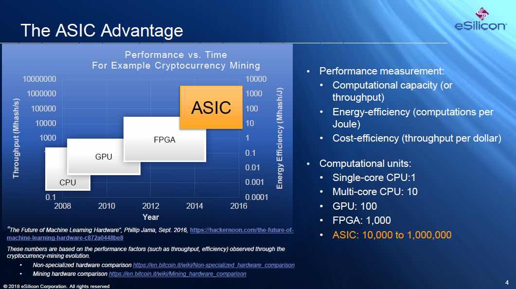
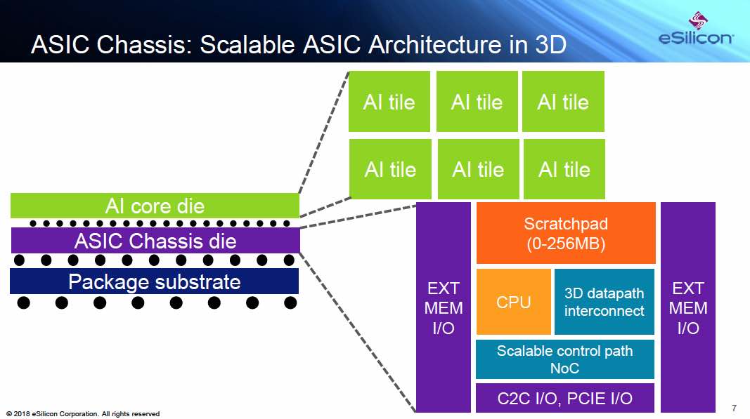
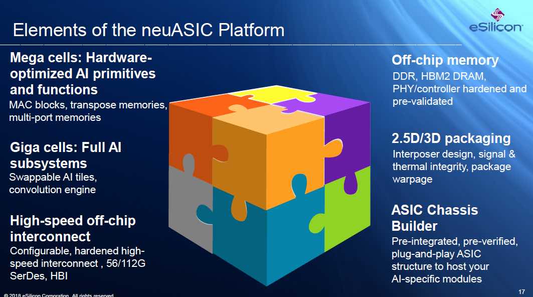


Comments
One Reply to “Being Intelligent about AI ASICs”
You must register or log in to view/post comments.