







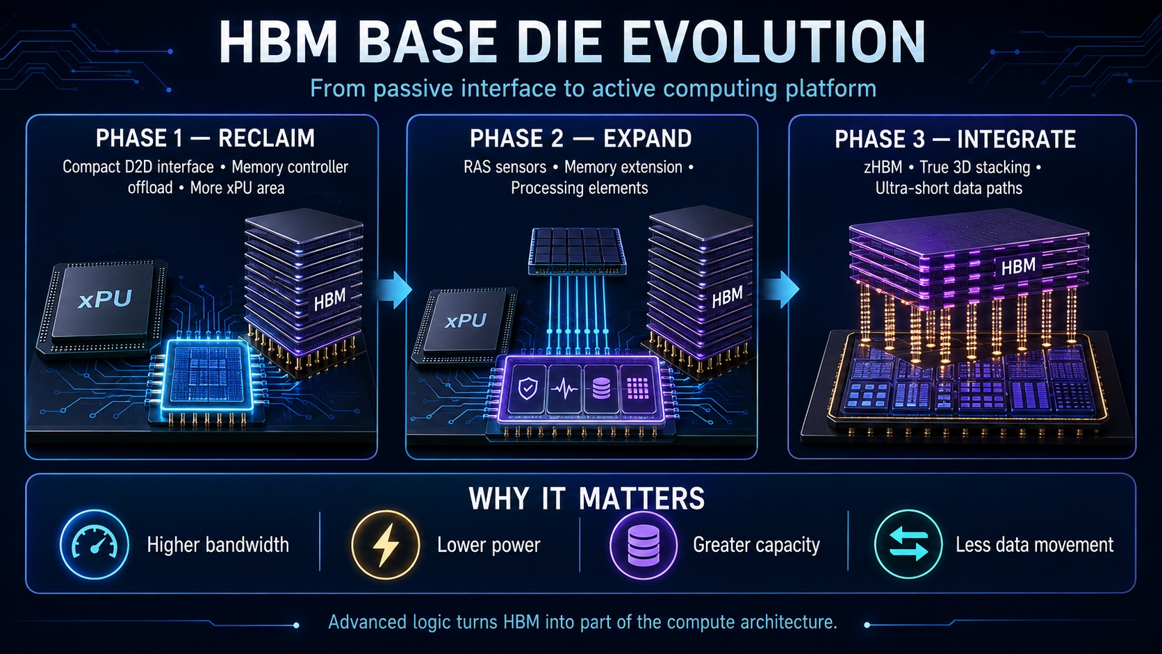
Samsung’s Hot Chips 2026 presentation, “HBM Base Die: How HBM Will Evolve Using Advanced Logic Processes,” argues that the base die beneath a High Bandwidth Memory stack is about to become far more than a communications layer. Traditionally, an HBM base die mainly connects stacked DRAM dies to a GPU, TPU, or other processor and provides testing functions. Samsung envisions turning it into an active, customizable logic platform—first absorbing functions from the processor, then adding new capabilities, and ultimately enabling direct three-dimensional integration between memory and computing.
This transformation is being driven by bandwidth, power, and physical constraints. AI processors need ever-faster access to increasingly large amounts of memory, but conventional scaling is approaching several limits. Transistor improvements are slowing, processors are nearing maximum reticle size, and interposers cannot expand indefinitely. Within HBM itself, the number and pitch of through-silicon vias constrain bandwidth, while wider and faster physical interfaces consume more area and power. Although each transmitted bit is becoming more efficient, total interface power continues to rise as aggregate bandwidth grows.
Samsung’s pivotal change began with HBM4, whose base die uses an advanced 4-nanometer logic process rather than a conventional DRAM process. Better logic transistors reduce power, delay, and active area, narrowing the technological gap between the base die and the processor. This creates “custom HBM,” or cHBM: products that can share standardized DRAM stacks while tailoring base-die logic to a particular processor or workload.
The proposed roadmap has three phases. Phase One reclaims valuable processor area. A compact die-to-die interface replaces the large conventional HBM physical interface, shortening signal paths and improving energy efficiency. The memory controller can then move from the processor into the HBM base die. Samsung also proposes SRAM-based repair logic that can replace defective DRAM rows, potentially improving usable capacity and manufacturing yield. Shrinking the interface, however, raises power density, so heat-path blocks are introduced to conduct heat through the stack and reduce peak temperatures.
Phase Two exploits silicon that would otherwise be used mostly for routing. The base die could incorporate thermal, voltage, process, and aging sensors for real-time reliability, availability, and serviceability monitoring. On-die testing and pattern generation could improve fault coverage and yield. Dedicated controllers and interfaces could connect HBM directly to external memory, providing greater capacity with better bandwidth and latency than PCIe-based expansion. Processing elements could also move into the base die, reducing data movement across the interposer. Samsung calls this compute-enhanced form “advanced HBM,” or aHBM.
Phase Three proposes zHBM, a true 3D architecture in which processor logic sits vertically beneath the DRAM stack. Distributed connections would shorten internal data paths and eliminate conventional high-power serial interfaces. Samsung estimates that eliminating this overhead could reduce HBM I/O power by about 70 percent. Achieving zHBM would require wafer-on-wafer assembly, hybrid copper bonding, and a unified design and verification process spanning processor logic, DRAM, packaging, timing, power, signal integrity, and testing.
Why does this matter? Modern AI performance increasingly depends not only on computing capacity but on moving and storing data efficiently. Longer context windows, larger key-value caches, and memory-intensive inference make bandwidth, capacity, and energy central system constraints. If Samsung’s roadmap succeeds, HBM will cease to be a relatively passive component selected after processor design. It will become part of the computing architecture itself.
Bottom line: That shift could yield faster AI systems without relying solely on larger processors or more power. It could improve yield, free expensive processor area, reduce data movement, expand capacity, and support workload-specific acceleration. Just as importantly, it would change industry relationships: memory vendors, processor designers, foundries, and packaging specialists would need to co-design products much earlier. The base die therefore represents both a technical opportunity and a strategic battleground. Whoever controls its logic, interfaces, and integration may influence how the next generation of AI systems is built—and how efficiently it scales.
Source: Sangwook Han, Samsung Memory Business, “HBM Base Die: How HBM Will Evolve Using Advanced Logic Processes,” August 23, 2026.
Also Read:
Crescent Island: Turning Memory Capacity into Agentic AI Throughput
Intel Diamond Rapids: Building Xeon Up, Out, and Through Silicon
Intel Wildcat Lake: Right-Sizing Silicon Without Sinking Performance
Share this post via:



CEO Interview with Charlie Cheng of CEO of TeRAM