In early April, Gabriele Saucier kicked off Design & Reuse’s IPSoC Silicon Valley 2021 Conference. IPSoC conference as the name suggests is dedicated to semiconductor intellectual property (IP) and IP-based electronic systems. There were a number of excellent presentations at the conference. The presentations had been categorized into eight different subject matter tracks. The tracks were Advanced Packaging Solution and Chiplet, Analog and Memory Blocks, Design and Verification, Interface IP, Security Solutions, Automotive IP and SoC, Video IP and High-Performance Computing.
Semiconductor Packaging as a technology has garnered lot of investment and attention for many years now. We have had various innovations over the years including flip-chip, silicon interposer, 2.5D, 3D, chip scale packaging and wafer level packaging. Many of these advances were driven by the need to overcome device performance limitations, signal-integrity issues, form-factor constraints and/or simply market acceptance price points. So, the “advanced packaging solution and chiplet” track piqued my interest and I listened in on some of the presentations.
One of the presentations I listened to was titled “Enabling Next Generation Silicon In Package Products” and was presented by Tony Pialis, the CEO of Alphawave IP, Inc.
There is a long history of successful system-in-a-package (SiP) products launched by different companies. One reason for going the SiP route is faster time to market (TTM). By mixing and matching IP that pre-exist in different process technologies, the time, effort and cost of having to port the different IP blocks to the same process technology is avoided. System-in-a-package interchangeably referred to as silicon-in-package is not a new concept.
So, why was Tony’s presentation under the Advanced Packaging track? This blog addresses that question through salient points gathered from Tony’s talk. For complete details, please register and listen to Tony’s entire talk.
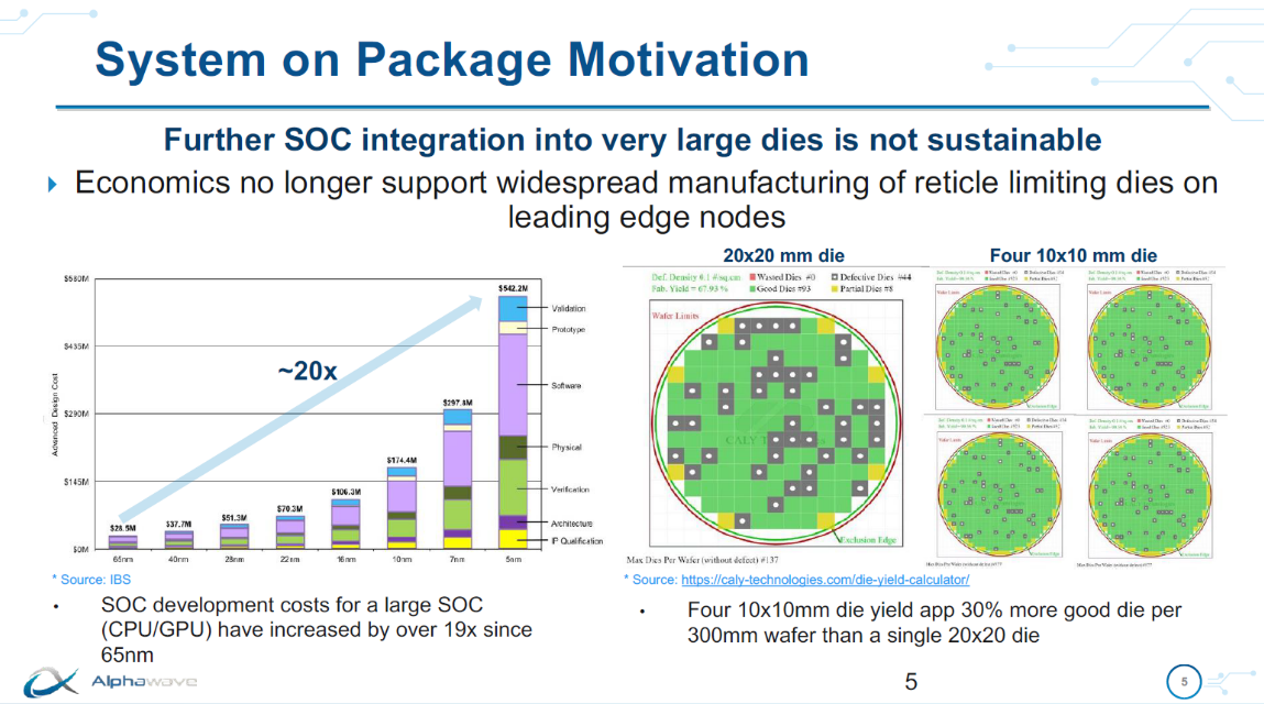
Next generation products are expected to see broader and faster adoption of SiP. As sub-10nm process node becomes main stream, two strong reasons for SiP adoption come into play (see Figure 1). The first reason: System-on-a-chip (SoC) development cost crossing the $500M mark. That is a 20X increase compared to the cost of developing an SoC in 65nm process node. The second reason revolves around die yield and number of good dies per wafer. The yield rate is better for smaller dies. Here in lies the opportunity to benefit economically, if all technical challenges can be overcome.
Figure 1: Opportunity from an Economic Perspective

Technical Challenges:
Achieving the economic benefits requires disintegrating an SoC die into smaller dies. In this context, these smaller dies are being termed chiplets. Simplistic definition of a chiplet: a die that holds a functional circuit block. But this approach of partitioning into chiplets introduces many challenges. A number of nanometer pitch wires that were on-chip now turn into package-level interconnects, thereby introducing signal integrity issues. longer latencies, increased power and test complexities.
Technology Solutions:
The good news is that manufacturing capabilities in the form of silicon interposer, through-silicon-vias and chip scale packaging technologies already exist to enable chiplets integration. The focus is now on chiplet interfaces to eliminate the signal integrity, latency and power issues. At a basic level, partitioning of an SoC leads to chiplets that are primarily logic bound, memory bound or I/O bound. The chiplet type determines what type of interface makes sense and what interface standards are available/supported.
Parallel interface implementations such as the Bunch of Wires (BoW) interface which is an Open Domain-Specific Architecture (ODSA) sub-committee supported standard, and the Advanced Interface Bus (AIB) interface which is an Intel/DARPA supported standard are well suited for use with logic bound chiplets.
The High Bandwidth Memory (HBM) interface standard, which is well established and in wide use is more suited for memory bound chiplets.
Serial interface implementations such as the XSR (extra short reach) and the USR (ultra short reach) interfaces are well suited for use with I/O bound chiplets.
In his presentation, Tony discusses lot of details in terms of supported speeds, latencies, power, bandwidth, etc., for each of these interface types. He delves deep into Alphawave IP’s DieCORE 112Gbps XSR interface IP and discusses ways of managing bit error rate (BER) performance.
If interested in benefiting from a chiplets implementation approach, I recommend you register and listen to Tony’s entire talk and then discuss with Alphawave IP on ways to leverage their different IP offerings for developing your products.
Also Read:
CEO Interview: Tony Pialis of Alphawave IP
Alphawave IP and the Evolution of the ASIC Business
Alphawave IP is Enabling 224Gbps Serial Links with DSP
Share this post via:


Comments
There are no comments yet.
You must register or log in to view/post comments.