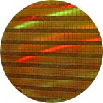
Once again industry professionals get duped! Tabloid journalism runs amok inside the semiconductor ecosystem! As if our industry does not face enough challenges, why are we wasting time on drivel like this? This is a TSMC 28nm wafer by the way and thousands of them are being shipped around the world, believe it.
… Read More
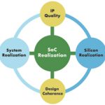
Atrenta/TSMC Soft-IP Alliance: 10 companies make the grade
Last May, Atrenta and TSMC announced the Soft-IP Alliance Program which uses SpyGlass and a subset of its GuideWare reference methodology to implement TSMC’s IP quality assessment program. TSMC requires all soft-IP providers to reach a minimum level of completeness before their IP is listed on TSMC online. Since TSMC … Read More
TSMC 28nm Yield Explained!
Yield, no topic is more important to the semiconductor ecosystem. After spending a significant part of my career on Design for Manufacturability (DFM) and Design for Yield (DFY), I’m seriously offended when semiconductor professionals make false and misleading statements that negatively affects the industry that … Read More
The Qualcomm PUT and The FABulous Year Ahead
Humor can arise in surprising ways and yet still be disguised to many. As I was researching Qualcomm the other day, I came upon the transcript of their last quarterly earnings and I had to laugh. In the midst of last summer’s European crises, when the Club Med (Greece, Italy, Spain and Portugal) Sovereign Debt was trying to be rolled… Read More
Tracking the Big Semiconductor Story of 2012
It’s just a matter of time – perhaps just a few months – before the greatest mystery of the semiconductor industry is revealed and the peaceful co-existence of the Fab vs Fabless world is blown apart. An arms race was started by Intel to challenge TSMC and Samsung on who would control not only the high valued processor but soon… Read More
GlobalFoundries Versus Samsung!
Some call it co-opetition (collaborative competition), some call it keeping your enemies close. Others call it for what it is, unfair competition and/or other types of legally actionable behavior. GlobalFoundries calls it“Fab Syncing”, which in reality will SINK their FABS!
“With this new collaboration, we are making one … Read More
Did Apple Influence AMD’s TSMC Foundry Switch?
During the weekend, I read two articles that highlighted Apple’s LCD supply chain build out and started to think of how this would look if Apple were to do the same on the x86 side of the ledger. The two articles, one related to Hitachi and Sony building a new 4” LCD for iphones and a more extensive one on Sharp building a new LCD for the iPAD3… Read More
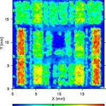
Physical Verification of 3D-IC Designs using TSVs
3D-IC design has become a popular discussion topic in the past few years because of the integration benefits and potential cost savings, so I wanted to learn more about how the DRC and LVS flows were being adapted. My first stop was the Global Semiconductor Alliance web site where I found a presentation about how DRC and LVS flows were… Read More
Synopsys Awarded TSMC’s Interface IP Partner of the Year
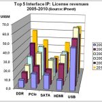
Is it surprising to see that Synopsys has been selected Interface IP partner of the year by TSMC? Not really, as the company is the clear leader on this IP market segment (which includes USB, PCI Express, SATA, DDRn, HDMI, MIPI and others protocols like Ethernet, DisplayPort, Hyper Transport, Infiniband, Serial RapidIO…). But,… Read More
3D Transistors @ TSMC 20nm!
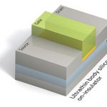
Ever since the TSMC OIP Forum where Dr. Shang-Yi Chiang openly asked customers, “When do you want 3D Transistors (FinFETS)?” I have heard quite a few debates on the topic inside the top fabless semiconductor companies. The bottom line, in my expert opinion, is that TSMC will add FinFETS to the N20 (20nm) process node in parallel with… Read More


