You are currently viewing SemiWiki as a guest which gives you limited access to the site. To view blog comments and experience other SemiWiki features you must be a registered member. Registration is fast, simple, and absolutely free so please,
join our community today!
            WP_Term Object
(
    [term_id] => 18
    [name] => Intel Foundry
    [slug] => intel
    [term_group] => 0
    [term_taxonomy_id] => 18
    [taxonomy] => category
    [description] =>
    [parent] => 158
    [count] => 466
    [filter] => raw
    [cat_ID] => 18
    [category_count] => 466
    [category_description] =>
    [cat_name] => Intel Foundry
    [category_nicename] => intel
    [category_parent] => 158
    [is_post] =>
)

WP_Term Object
(
    [term_id] => 18
    [name] => Intel Foundry
    [slug] => intel
    [term_group] => 0
    [term_taxonomy_id] => 18
    [taxonomy] => category
    [description] =>
    [parent] => 158
    [count] => 466
    [filter] => raw
    [cat_ID] => 18
    [category_count] => 466
    [category_description] =>
    [cat_name] => Intel Foundry
    [category_nicename] => intel
    [category_parent] => 158
    [is_post] =>
)
The successful transition to a new fabrication process from development to high volume manufacturing requires a collective, collaborative effort among process engineers, equipment manufacturers, and especially, chemical suppliers. Of particular importance is the chemistry of the photoresist materials and their interaction… Read More
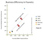
While there is a lot of excitement around the semiconductor shortage narrative and the fabs all being full, both 200mm and 300mm, there is one big plot hole and that is the FinFET era.
Intel ushered in the FinFET era only to lose FinFET dominance to the foundries shortly thereafter. In 2009 Intel brought out a 22nm FinFET wafer at the… Read More
Dan is joined by Dr. Walden Rhines. Dan and Wally explore Intel’s re-entry to the foundry business. What is different this time and the implications of a worldwide supply chain are just some of the topics discussed in this far-reaching discussion of what lies ahead for the semiconductor industry.
The views, thoughts and … Read More
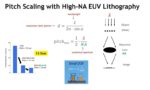
A great deal has been written of late about the demise of Moore’s Law. The increase in field-effect transistor density with successive process nodes has slowed from the 2X every 2 1/2 years pace of earlier generations. The economic nature of Moore’s comments 50 years ago has also been scrutinized – the reduction in cost per transistor… Read More
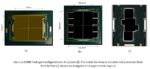
The evolution of low-cost heterogeneous multi-chip packaging (MCP) has led to significant system-level product innovations. Three classes of MCP offerings have emerged:
- wafer-level fan-out redistribution, using reconstituted wafer substrates of molding compound as the surface for interconnections between die (2D)
…
Read More
– Intel announced 2 new fabs & New Foundry Services
– Not only do they want to catch TSMC they want to beat them
– It’s a very, very tall order for a company that hasn’t executed
– It will require more than a makeover to get to IDM 2.0
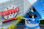
Intel not only wants to catch TSMC but beat them at their own … Read More
Intel made a big splash on March 23, 2021 by doubling down on manufacturing with the creation of Intel Foundry Services (IFS). The big announcement was supported by potential customers such as Qualcomm, Cisco, Ericsson, Google, Amazon, Microsoft, and IBM. With an accompanying $20B investment, the EDA and equipment industries,… Read More
In January I presented at the ISS conference a comparison of Intel’s, Samsung’s and TSMC’s leading edge offerings. You can read a write-up of my presentation here.
With the problems going on at Intel, that article generated a lot of interest in the investment community, and I have been holding a lot of calls with analysts who are trying… Read More
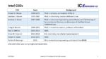
New Intel CEO Pat Gelsinger is not wasting any time in changing the course of the largest semiconductor company the world has ever seen. Today he announced the IDM 2.0 strategy which will better leverage Intel’s manufacturing abilities. There is a lot to talk about here but let’s focus on the new Intel Foundry Services because the… Read More
Dan takes an in-depth look at Intel with Stacy Rasgon, Managing Director and Senior Analyst, U.S. Semiconductors at Bernstein Research. Stacy is an unusual semiconductor analyst as he holds a Ph.D. in chemical engineering from MIT. His substantial technical knowledge allows for a deep dive on Intel that you will find refreshing… Read More