You are currently viewing SemiWiki as a guest which gives you limited access to the site. To view blog comments and experience other SemiWiki features you must be a registered member. Registration is fast, simple, and absolutely free so please,
join our community today!
WP_Term Object
(
    [term_id] => 20
    [name] => Samsung Foundry
    [slug] => samsung-foundry
    [term_group] => 0
    [term_taxonomy_id] => 20
    [taxonomy] => category
    [description] =>
    [parent] => 158
    [count] => 135
    [filter] => raw
    [cat_ID] => 20
    [category_count] => 135
    [category_description] =>
    [cat_name] => Samsung Foundry
    [category_nicename] => samsung-foundry
    [category_parent] => 158
    [is_post] =>
)
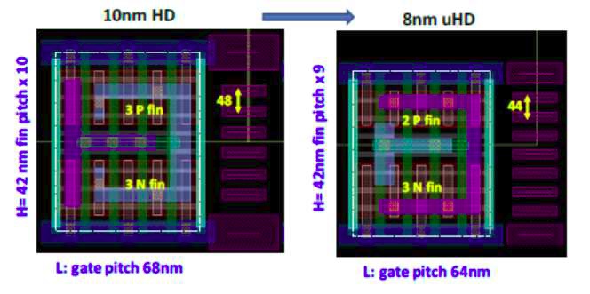
I got a tip sheet today for the upcoming 2018 Symposia on VLSI Technology & Circuits to be held June 19th through 21st in Honolulu, Hawaii. There is some interesting information on Samsung’s 10nm, 8nm and 7nm processes in the tip sheet:… Read More
Samsung throws further gas on the fire of weak handset and CAPEX not set but will be down versus 2017. Samsung reported revenues of KRW 60.56 Trillion and KRW 15.64 Trillion operating profit ($56B and $15B). Chips accounted for whopping KRW 11.55 Trillion in operating profit on revenues of KRW 20.78 Trillion ( $11B and $19B)….a… Read More
There is a report in the Seoul Economic Daily that Samsung has completed development of their 7nm process using EUV and that production will begin in June. What is claimed in the report is:
- The process is installed in the Hwaseong S3 Fab
- Samsung has more than 10 EUV systems installed
- Production starts in June with Qualcomm, Xilinx,
…
Read More
The most viewed blogs I write for SemiWiki are consistently blogs comparing the four leading edge logic producers, GLOBALFOUNDRIES (GF), Intel, Samsung (SS) and TSMC. Since the last time I compared the leading edge new data has become available and several new processes have been introduced. In this blog I will update the current… Read More
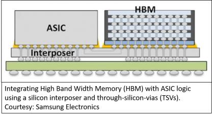
High Bandwidth Memory (HBM) systems have been successfully used for some time now in the network switching and high-performance computing (HPC) spaces. Now, adding fuel to the HBM fire, there is another market that shares similar system requirements as HPC and that is Artificial Intelligence (AI), especially AI systems doing… Read More
I was invited to give a talk at the ISS conference on the Impact of EUV on the Semiconductor Supply Chain. The ISS conference is an annual gathering of semiconductor executives to review technology and global trends. In this article I will walk through my presentation and conclusions.… Read More
I remember the days of the IDM (integrated device manufacturer). For me, it was RCA, where I worked for 15 years as the company changed from RCA to GE and then ultimately to Harris Semiconductor. It’s a bit of a cliché, but life was simpler then, from a customer point of view at least. RCA did it all. We designed all the IP, did the physical… Read More
For Halloween this week we thought it would be appropriate to talk about things that strike fear into the hearts of semiconductor makers and process engineers toiling away in fabs. Do I want to do multi-patterning with the huge increase in complexity, number of steps, masks and tools or do I want to do EUV with unproven tools, unproven… Read More
This week Dr. Eric Esteve, Dr. Bernard Murphy, and I will be blogging live from Arm TechCon. It really looks like it will be a great conference so you should see some interesting blogs in the coming days. One of the topics I am interested in this year is foundation IP and I will tell you why.
During the fabless transformation of the semiconductor… Read More
Being the number one EDA and the number one IP company does have its advantages and the resulting foundry relationships are a clear example. One of the DAC traditions that I truly enjoy is the Synopsys foundry breakfasts. Not only does Synopsys welcome scribes, they reserve a table up front for us and Synopsys CEO Aart de Geus has been… Read More


Solving the EDA tool fragmentation crisis