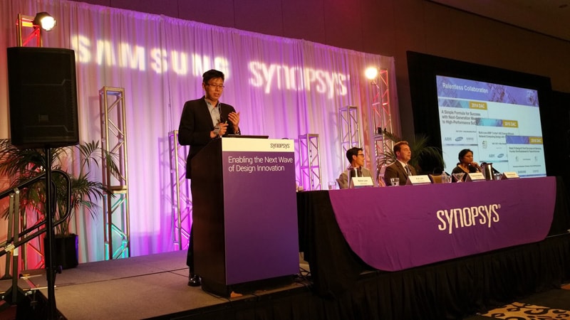
I’m a user of many Samsung products as my family has Samsung Galaxy smart phones and my MacBook Pro uses Samsung SSD for storage, so at DAC I attended a breakfast panel with presenters from Samsung, Synopsys and Qualcomm. This was the second day of DAC and they served us breakfast, and with the big names on the panel the room was crowded with engineers all wanting to hear about the Samsung roadmap and how Qualcomm designed their latest SoC.


KK Lin of Samsung Foundry presented first, and he reminded us that Samsung has made the Foundry business separate from the parent company. Their foundry claims first to market for 14nm FinFET technology, and now has delivered 1 million wafers. Their 10nm process node started limited production in late 2016. Right now Samsung Foundry is qualified and certified at 10nm with EDA tools form Synopsys, while Qualcomm hails as an early customer.
Here’s the Samsung Foundry process roadmap:
2017 – 8Lpp, 10LPU, 14LPU
2018 eMRAM, 7LPP with EUF
2019 5LPP, 6LPP, 18FDS
2020 4LPP, eMRAM
Co-optimizing process and tools has been the approach taken for several nodes now. Markets for these leading edge FinFET technologies are: GPU, Network, Mobile, Auto, Consumer, IoT. There are five different fab locations around the world for Samsung Foundry, and they are also quite active in packaging with:
- SiP
- Package on package
- Silicon interposer
- Si-less interposer
At the 4nm process node expect to see something called MBCFET (Multibridge-channel FET).

Second to present was Thomas Andersen, a Group Director at SNPS, and he shared that their tools for 10nm are certified now, while the 8LPP/7LPP are in a readiness phase. TheirIC Validatortool is ready for 8LPP. For a design flow they use the Lynx system.
With the 7LPP process you can expect a single pattern EUV process, making it a bit simpler to design with. On the EDA side the logic synthesis tool DesignCompiler is deeply physical and handles issues like:
- 31 layer promotion
- Resistive shielding
- Parametric OCV
- Correlation with IC Compiler
- Faster run times with a 4M instance capacity
For place and route the IC Compiler II tool has zero margin timing correlation, integrated SPICE-correlated EM analysis, and has optimization for total power and low power. With all of the new layout rules for the smallest process nodes it does make P&R tools run more slowly now compared to previous nodes.
Related blog –Polishing Parallelism
On the static timing analysis front the PrimeTime tools now supports ultra-low voltages (ULV). Even the IC Compiler II tool is using the PrimeTime engine inside, leading to no over design and reduced ECO cycles.
With physical DRC you can use either In-Design IC Validator or standalone IC Validator.

Our final presenter wasMamta Bansal from Qualcomm, Senior Director of Engineering. They announced the Snapdragon 835 SoC used in mobile devices, fabricated at the 10nm node with Samsung Foundry. This SoC is the first 10nm to ship in volume production, and it’s die size is 35% smaller, using 25% less power, while delivering a 25% faster GPU than prior generation. You could use the 835 for Virtual Reality or Augmented Reality because it supports a 360 degree camera or a 3D camera.
The IC layout process at 10nm is too complex for full-custom, so they use a structured flow instead, using even and odd poly cells for boundaries to simplify. Some layers are 2, 3 or 4 patterns, and a colorless flow was used. M1 is a triple color layer. The power mesh uses only one color. IC Compiler does all of the legal coloring and swapping automatically, making IC design much easier. No changes in the 10nm P&R design flow compared to 14nm.
They saw up to a 4% area improvement using ICC II, while meeting both power and timing closure.
At 10nm it was a challenge to do cell characterization, and they used the SiliconSmart tool. Adding more conditions improved the accuracy in SiliconSmart.
Bottom line, 10nm design is ready with Synopsys tools and Samsung Foundry.
Q&A Session
Q: What is the size of Samsung Foundry?
A: We are #2 in revenue.
Q: When is the ASML talk?
A: In the Samsung booth at 10:45AM
Q: What are the challenges expected just beyond 10nm?
A: Routability, zero margin. 7EUV reduces complexity through 1 pattern layer.
Q: How should we manage temperature effects in SoCs?
A: This is really a system level issue, we can create thermal models then perform a hierarchical analysis (chip, package board). Thermal aware tools are needed, and then designing chips that throttle the clock to keep power in spec with on-chip sensors.
Q: What challenges are there to a foundry to support RF and NVM?
A: Our 28nm process supports RF now, and the challenge is in creating the high frequency models. EMRAM is new for us.


Is Intel About to Take Flight?