You are currently viewing SemiWiki as a guest which gives you limited access to the site. To view blog comments and experience other SemiWiki features you must be a registered member. Registration is fast, simple, and absolutely free so please,
join our community today!
WP_Term Object
(
    [term_id] => 20
    [name] => Samsung Foundry
    [slug] => samsung-foundry
    [term_group] => 0
    [term_taxonomy_id] => 20
    [taxonomy] => category
    [description] =>
    [parent] => 158
    [count] => 135
    [filter] => raw
    [cat_ID] => 20
    [category_count] => 135
    [category_description] =>
    [cat_name] => Samsung Foundry
    [category_nicename] => samsung-foundry
    [category_parent] => 158
    [is_post] =>
)
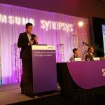
I’m a user of many Samsung products as my family has Samsung Galaxy smart phones and my MacBook Pro uses Samsung SSD for storage, so at DAC I attended a breakfast panel with presenters from Samsung, Synopsys and Qualcomm. This was the second day of DAC and they served us breakfast, and with the big names on the panel the room was… Read More
At Semicon West last week I attended presentations by Soitec and CEA Leti, and had breakfast with CEA Leti CEO Marie Semeria, key members of the Fully Depleted Silicon On Insulator (FDSOI) ecosystem. I have also seen some comments in the SemiWiki forum lately that make me believe there is some confusion on the roles of different companies… Read More
I have previously published analysis’ converting leading edge logic processes to “standard nodes” and comparing standard nodes by company and time. Recently updated details on the 7nm process node have become available and in this article, I will revisit the standard node calculations and trends.… Read More
For many year 2D NAND drove lithography for the semiconductor industry with the smallest printed dimensions and yearly shrinks. As 2D NAND shrunk down to the mid-teens nodes, 16nm, 15nm and even 14nm, the cells became so small that there were only a few electrons in each cell and cross-talk issues made further shrinks very difficult… Read More
Samsung recently held a meeting where they laid out a detailed roadmap for their foundry business. On Tuesday June 1st, Daniel Nenni and myself had an interview with Kelvin Low, senior director of foundry marketing and business development to discuss the details of Samsung’s plans.… Read More
Last week Intel held a manufacturing day where they revealed a lot of information about their 10nm process for the first time and information on competitor processes continues to slowly come out as well. I thought it would be useful to summarize what we know now, especially since some of what Intel announced was different than what… Read More
For an industry that drives improvement at an exponential rate it is funny how often something old is new again. Intel went into high volume production on 22nm in 2011, and TSMC and Samsung have both had 20nm technologies in production for several years. And yet, recently we have seen renewed interest in 22nm. GLOBALFOUNDRIES has… Read More
Yesterday I attended Intel’s manufacturing day. This was the first manufacturing day Intel has held in three years and according to Intel their most in depth ever.
Nodes must die
I have written several articles comparing process technologies across the leading-edge logic producers – GLOBALFOUNDRIES, Intel, Samsung… Read More
As you all know I’m a big fan of the ASIC business dating back to the start of the fabless semiconductor transformation where anybody could send a design spec to an ASIC company and get a chip back. The ASIC business model also started the smart phone revolution when Samsung built the first Apple SoCs for the iPhones and iPads.
Today … Read More
The annual SPIE Advanced Lithography Conference kicked off last night with vendor sponsored networking events and such. SPIE is the international society for optics and photonics but this year SPIE Advanced Lithography is all about the highly anticipated EUV technology. Scotten Jones and I are at SPIE so expect more detailed… Read More

Solving the EDA tool fragmentation crisis