You are currently viewing SemiWiki as a guest which gives you limited access to the site. To view blog comments and experience other SemiWiki features you must be a registered member. Registration is fast, simple, and absolutely free so please,
join our community today!
WP_Term Object
(
    [term_id] => 89
    [name] => FinFET
    [slug] => finfet
    [term_group] => 0
    [term_taxonomy_id] => 89
    [taxonomy] => category
    [description] =>
    [parent] => 0
    [count] => 233
    [filter] => raw
    [cat_ID] => 89
    [category_count] => 233
    [category_description] =>
    [cat_name] => FinFET
    [category_nicename] => finfet
    [category_parent] => 0
    [is_post] =>
)
Tuesday July 9th was the first day the show floor was open at Semicon. The following is a summary of some announcements I attended and general observations.
AMAT Announcement
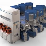
My day started with an Applied Materials (AMAT) briefing for press and analysts where they announced “the most sophisticated system they have ever released”.… Read More
Since the beginning of May eSilicon has announced the tape-out of three TSMC 7nm test chips. The first of these, a 7nm 400G Ethernet Gearbox/Retimer design, caught my eye and I followed up with Hugh Durdan, their vice president of strategy and products, to learn more about it. Rather than just respin their 56G SerDes, they decided… Read More
One of my favorite EDA disruptions is the Siemens acquisition of Mentor, pure genius. Joe Sawicki now runs the Mentor IC EDA business for Siemens so we will be seeing him at more conferences and events than ever before. Joe did a very nice keynote at the recent U2U conference that I would like to talk about before we head to the 56thDAC… Read More
Designing with advanced-nodes FinFETs such as 7nm node involves a more complex process than prior nodes. As secondary physical effects are no longer negligible, the traditional margin-based approach applied at various design abstraction levels is considered ineffective. Coupled with the increase of device counts, failing… Read More
Perhaps the most innovative and effective Extension implant does not involve an implant at all, but is instead an etch followed by a selective epitaxial deposition.
In this Extension fabrication methodology the Source/Drains regions in a planar device are etched away in the normal fashion to accommodate the replacement Source/Drain… Read More
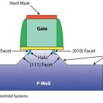
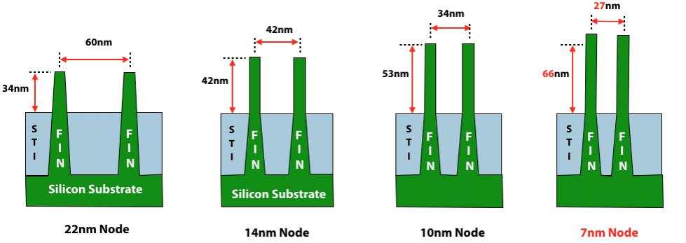
The problem of traditional FinFET Extension Implant doping concerns the awkward 3-dimensional structure of the fin. Because the Extension Implant defines the conductive electrical pathway between the Source/Drains and the undoped channel portion of the fin, it is essential that the fin be uniformly doped all three of its surfaces… Read More
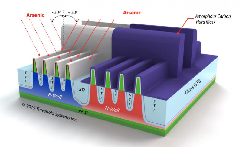
The use of hard masks instead of photoresist for the Extension implant is an effective way to optimize the amount of dopant that is retained along the fin sidewalls for those fins that border along photoresist edges (as discussed in Part 1 of this series).
However, hard masks do nothing to address the dominant problem driving steeper… Read More
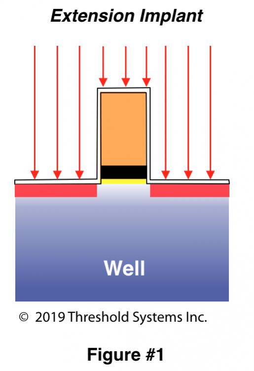
The 3D character of FinFET transistor structures pose a range of unique fabrication problems that can make it challenging to get these devices to yield. This is especially true for the all-important Extension implant that is put in place just prior to the nitride spacer formation.
The Extension implant is a central component of… Read More
This year TSMC did a FinFET victory lap with the success of 16nm, 12nm, 10nm, and 7nm. It really is well deserved. Even though TSMC credits the ecosystem and customers, I credit TSMC and their relationship with Apple since it has pushed us all much harder than ever before. TSMC CEO C.C. Wei summed it up nicely in his keynote: Innovation,… Read More
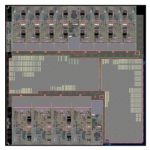
Physical IC design is a time consuming and error prone process that begs for automation in the form of clever EDA tools that understand the inter-relationships between logic synthesis, IC layout, test and sign-off analysis. There’s even an annual conference called ISPD – International Symposium on Physical Design… Read More


TSMC CoWoS versus Intel EMIB Semiconductor Packaging