You are currently viewing SemiWiki as a guest which gives you limited access to the site. To view blog comments and experience other SemiWiki features you must be a registered member. Registration is fast, simple, and absolutely free so please,
join our community today!
As the number one 56thDAC supporting portal we will publish what’s happening in the conference, on the exhibit floor, and outside activities. The SemiWiki bloggers will be out in full force with live coverage and behind the scenes looks. Remember, SemiWiki bloggers are actual semiconductor professionals with hundreds… Read More
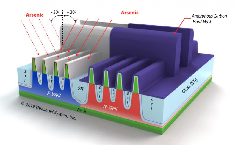
Part 4 of this series discussed how a transistor Extension could be fabricated in a planar device without using an implant operation, and is instead formed using a preferential etch followed by a selective epitaxial deposition. This final installment of the series will present the formation of an Extension in a FinFET transistor… Read More
Hello Cambridge, Grenoble, Stockholm, Moscow, Munich and Amsterdam
Our 2019 global symposiums and workshops have been hugely successful in promoting the RISC-V ISA and fostering expansive collaboration within the open-source community. It’s invigorating to see how the worldwide semiconductor ecosystem is energized and… Read More
Perhaps the most innovative and effective Extension implant does not involve an implant at all, but is instead an etch followed by a selective epitaxial deposition.
In this Extension fabrication methodology the Source/Drains regions in a planar device are etched away in the normal fashion to accommodate the replacement Source/Drain… Read More
Reason number ONE:The next five DACs will be in San Francisco and this will probably be the last one held in Las Vegas so you absolutely do NOT want to miss it. One of my most memorable DACs was in Las Vegas in 1985. My wife came with me for our second honeymoon and, by definition, it was just that, a honeymoon. This year we will probably spend… Read More
Having just completed a cloud evaluation for SemiWiki I can tell you why eSilicon chose Google. Simply put, they are working harder to get cloud business. Google ($4B) is the number five cloud provider behind Microsoft ($21.2B), Amazon ($20.4B), IBM ($10.3B) and Oracle ($6.08B). There is a lot of money in the cloud and a lot more … Read More
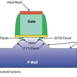
The problem of traditional FinFET Extension Implant doping concerns the awkward 3-dimensional structure of the fin. Because the Extension Implant defines the conductive electrical pathway between the Source/Drains and the undoped channel portion of the fin, it is essential that the fin be uniformly doped all three of its surfaces… Read More
The use of hard masks instead of photoresist for the Extension implant is an effective way to optimize the amount of dopant that is retained along the fin sidewalls for those fins that border along photoresist edges (as discussed in Part 1 of this series).
However, hard masks do nothing to address the dominant problem driving steeper… Read More
Methodics has been a key player in IP management for over 10 years. In this section, Methodics shares their history, technology, and their role in developing IP Lifecycle Management (IPLM) solutions for the electronics industry.
Methodics is recognized as a premier provider of IP Lifecycle Management (IPLM) and traceability… Read More
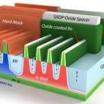
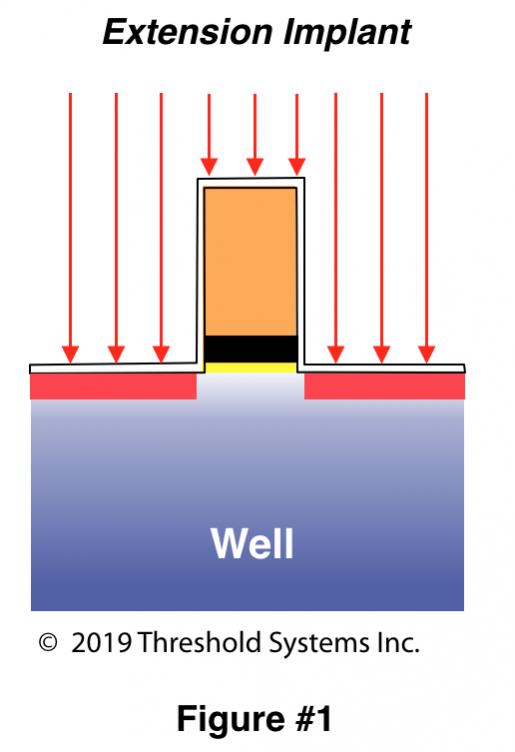
The 3D character of FinFET transistor structures pose a range of unique fabrication problems that can make it challenging to get these devices to yield. This is especially true for the all-important Extension implant that is put in place just prior to the nitride spacer formation.
The Extension implant is a central component of… Read More


Podcast EP357: How Gonka is Changing the Way AI is Accessed with David Liberman