





Array
(
    [content] => 
    [params] => Array
        (
            [0] => /forum/threads/the-truth-behind-huaweis-1-4nm-logicfolding-claim.25199/
        )

    [addOns] => Array
        (
            [DL6/MLTP] => 13
            [Hampel/TimeZoneDebug] => 1000070
            [SV/ChangePostDate] => 2010200
            [SemiWiki/Newsletter] => 1000010
            [SemiWiki/WPMenu] => 1000010
            [SemiWiki/XPressExtend] => 1000010
            [ThemeHouse/XLink] => 1000970
            [ThemeHouse/XPress] => 1010570
            [XF] => 2031070
            [XFI] => 1060170
        )

    [wordpress] => /var/www/html
)

The Truth Behind Huawei's 1.4nm LogicFolding Claim

Daniel Nenni

Founder
Staff member
The day of March 25th was an interesting one. At an IEEE conference, Huawei presented a paper and a set of slides on what it thinks is its next era of compute. With limited access to logic scaling, it is broadening the field, which makes sense. However, they also claim to jump ahead of everyone else in the world on few key metrics, and start calculating transistor density wrong, before we even saw that the research paper is written with AI.
There are questions to answer.

[00:00] Huawei 14A scaling overview
[00:14] Introduction to Tau Scaling [00:44] LogicFolding architecture concepts
[02:18] Huawei 14A density targets
[03:09] Tau Scaling physics principles
[09:21] LogicFolding interconnect mechanics
[10:48] AI academic writing patterns
[11:16] Stacking thermal management challenges
[15:24] Sub-micron LogicFolding specifications
[23:44] Huawei 14A density metrics
[33:16] 3D logic thermal limitations
[38:43] HBM logic stacking research
[43:05] Advanced bonding process yield
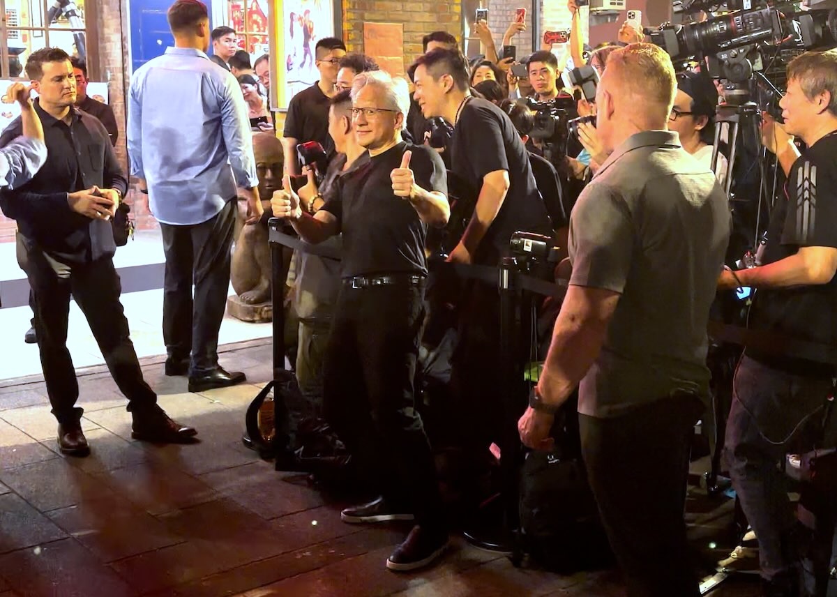
 

Huang Renxun, discussing Huawei's "Tao Law," stated that it involves overcoming non-threatening challenges and maintaining TSMC's ten-year lead.​


NVIDIA CEO Jensen Huang hosted a trillion-dollar banquet today. In an interview, he responded for the first time to Huawei's proposed new semiconductor law, "Tao," stating that it is indeed a breakthrough for Huawei, but does not pose a threat to TSMC , because TSMC has been developing technologies such as die stacking, 3D packaging, and hybrid bonding for nearly a decade.

Recently, Huawei's "Tao Law" has been the subject of much discussion in China's semiconductor industry. It focuses on improving chip performance and transistor density through 3D stacking, advanced packaging, and architecture integration without relying on EUV extreme ultraviolet light equipment. It even claims that it can achieve computing power similar to 1.4 nanometer level in the future, which has aroused market attention to whether it may challenge TSMC's existing technological advantages.

In response, Huang Renxun stated that Huawei, through technologies such as die stacking and hybrid bonding, can indeed increase the number of transistors by two, three, or even four times without further miniaturization processes, making it a very good technology.

However, he also emphasized that TSMC has been deeply involved in the relevant field for many years and its technology is already very advanced. Therefore, although Huawei's development is noteworthy, it will not pose a threat to TSMC.

In fact, TSMC has been continuously strengthening its CoWoS, SoIC, and advanced packaging capabilities in recent years, becoming a key component in AI GPUs and high-performance computing chips. The market generally believes that products from companies such as Nvidia's Blackwell and Rubin platforms, as well as those from AMD and Apple, heavily rely on TSMC's advanced packaging capabilities.

The outside world believes that Huawei's "Tao Law" reflects the strategic shift of China's semiconductor industry towards a "non-process miniaturization" route under US sanctions and EUV equipment restrictions. It hopes to make up for the gap in advanced processes through 3D IC, Chiplet, and system integration.


Back
Top