 According to the IEEE Std 1012-2012, verification is the acknowledgement that a product is in satisfactory condition by meeting a set of rigorous criteria. [3] Transistor-level verification involves the use of custom libraries and design models to achieve ultimate performance, low power, or layout density. [2] Prediction of accurate transistor behavior, within its surroundings, is the main challenge of this verification. For a while, all circuit designers did transistor-level verification. However, implementation of isolated, gate-level standard cells and thoroughly, detailed libraries caused a majority of designers to abandon it. [1] With recent technological advancements in transistor designs, new challenges have increased a number of designers to look back into transistor-level, verification tools.
Verification challenges are organized within three spheres of influence: smaller geometry, new devices, and variability. As transistors have moved to smaller and smaller geometries, VLSI designers have started to run into problems at atomic levels. Bruce McGaughy, CTO and Senior VP of ProPlus Design Solutions has stated, “In previous generations you had hundreds or thousands of atoms in the length of a channel but today it is down to tens,” [1]. In CMOS transistors, dopant atoms are fused into the silicon crystal to improve conductivity. The significant reduction in the amount of dopant atoms a transistor channels increases the threshold voltage. Along with less conductivity and increased threshold voltage, interconnects, wires connecting transistors, becomes another challenge. [1] In modern technologies, wires are more narrow, which increases resistance, to keep the design area to a minimum, the wires are closely packed, creating a capacitance due to voltage potential across them. It is noted that the variations in resistance and capacitance appear in every stage of the fabrication processes. However, as the processes shrink, the sensitivity to these variations increases, which makes it necessary to monitor more variables than previously needed.
A good example would be moving from 90nm to 14nm. Hany Elhak, Director of Product Management for Circuit Simulation and Library Characterization at Cadence Design Systems, noted, “At 90nm, analysis was only required for very sensitive analog blocks.” However, with small nodes like 14nm, variation analysis is required Standard Operating Procedures (SOP), even for digital designs. Transistors use thermal vibrations in the doped-silicon lattice to create channels. At smaller nodes, the thermal vibrations needed to activate the transistor increases, which amplifies the Electromigration (EM), ageing, the degradation of a MOS transistor over time [1]. Given these added variables, designers are now required to produce accurate voltage waveforms and current waveforms in order to verify factors such as power and thermal effects.
Layouts have also become a factor of smaller geometries, due to effects, such as leakage that affect nearby components. In previous generations of CMOS technologies, all of the transistors had an identical industry standard, a MOSFET (Metal-Oxide Semiconductor Field-Effect Transistor). It is a four terminal device, with the fourth terminal (body or substrate) connected to the source terminal. The layout of the chip design caused little variation, because the simplicity of the MOSFET geometry. Now with new types of geometries for smaller transistors (e.g. FinFet), the layout designs around the transistor may not be as identical as before. Different patterns from the layouts have to be taken into consideration in simulations.
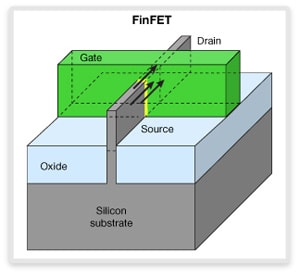
As we make the transition from planar transistors to FinFETs, a new BSIM (Berkeley Short-channel IGFET Model) model is needed in order to properly run the simulations required to ensure a proper functioning circuit. BSIM models are equation based models that are developed at UC Berkeley and supported by CMC (Compact Model Coalition). In order to run the simulations, these models are imported into your design in SPICE. In addition, the transition from planar transistors to FinFETs means more simulation computations. Ravi Subramanian, GM for the analog/mixed-signal group at Mentor Graphics, illustrates that “complexity is measured by the number and type of equation in these models. Going from planar to FinFET, the modeling complexity has increased by over 100X in terms of the raw number of computations required per transistor. That means that for every transistor, you need to do 100X more computations.” [1] The FinFET is one of the factors that adds to the complexity of the simulations. With the channel between source and drain shortened, leakage and Drain-Induced Barrier Lowering (DIBL), a change in threshold voltage and output conductance due to drain voltage, are some of the known negative effects of sub 50nm transistors. The FinFET is a 3D device with the gate wrapped around the channel, which mitigates DIBL and leakage. With the increase electron control, more charge can flow through the inversion region of the channel as the gate switches. The charge variation of the FinFET makes modeling more difficult, because of the changes in the depletion region of the IV curve. With traditional MOSFET devices, variation in the IV curve are most significant to simulations. Now VLSI designers need to take into account the charge variation of the smaller transistor as well as the IV characteristics. [1].
Moreover, the 3D layout has a rather negative impact on the thermal dissipation of the transistor, due to the wire density and overall density of the transistor. The increased heat due to poor dissipation leads to faster degradation and less reliability. Degradation in newer chips can be seen in layout interconnects where their increasing lengths and slim thicknesses and depths, high current density and higher operating temperatures occur. Changes such as replacing aluminum with copper have been made to lessen these effects but electromigration is still a problem as everything is moving to newer and more advanced nodes. When a circuit is active and electrons flow, the electrons can cause damage due to the heat and pressure that they generate within the metal. With the ever increasing push to smaller nodes, this becomes much more important and requires analyzing, where in the past it was only required to analyze sensitive analog blocks and high power blocks used in automotive. [1]
Hot carrier injection (HCI) and bias temperature instability (BTI) also play a part in the degradation of devices. Hot carrier injection occurs when enough kinetic energy injects particles into parts of a circuit that they shouldn’t be in such as the gate dielectric. The displacement of these particles cause “threshold voltage changes and trans conductance degradation in the device” [1]. Bias temperature instability occurs between the silicon dioxide layer and the substrate which causes the absolute threshold voltage to increase which in turn leads to degradation within the device. Hot carrier injection and bias temperature instability are both things that now must be taken into consideration in the libraries. [1]
Process variation increases as the new devices decrease in size. The main contributors to process variation are oxide thickness and mask alignment. Oxide thickness is the insulating pad between the gate and the dopants. To improve performance or size, the oxide thickness is reduced, which would lead to leakage. Moreover, the device is very sensitive to the slightest change in sub-20 nm transistors. Randomness of the variation adds more difficulty to the process, as all devices are no longer equally affected.
In past design procedures, VLSI designers’ solution to variability was to add margins. Due to “the sensitivity to varying parameters”, an even further amount of margins must be added. [1] According to Yoann Courant, R&D Director in the Process Variability Group (PVG) of Silvaco, ‘Monte Carlo is the traditional approach for variation analysis, but it is becoming too costly as thousands of runs are needed in order to statistically converge to an acceptable precision.” [1] He suggests that advanced Monte Carlo techniques are needed to speedup to simulation runs. Monte Carlo is a computational algorithm that obtains numerical results through repetition of random sampling. Recently, Subramanian has noticed a movement to use statistical analysis reasonably. He states, “We are at the early days of this. People are looking at, and starting to use an approach called ‘The Design of Experiments’.” [1] Additionally, people are considering how many simulations are required to attain a good confidence interval for a given situation. If a VLSI designer has a set of measurements, an equal number of experiments relative to the amount of measurements is necessary. In turn, the experiments are used to attain a certain degree of confidence for the initial measurements. [1]
As circuit designers progress to ever smaller processes, margins for error will keep growing tighter and simulations will continue increase in complexity. However, advancements in parallel calculations within newer chips will keep performance increasing without shrinking the manufacturing processes, which adds further complexity to simulations. With the increase in complexity, the right level of model abstraction is the main challenge. Another challenge is to have the proper methodology that enables designers to move in and out between different levels of abstractions for different blocks. A solution to these challenges is SystemVerilog. Verilog is no longer an active standard and with a migration towards SystemVerilog, new features and enhancements to strengthen mixed-signal design and verification are undertaken. SystemVerilog has a higher level of abstraction with specific design intent, meaning VLSI designers have more control over the logic of the design. Additionally, the higher abstraction level allows the VLSI designer to switch between different design levels. VHDL and Verilog users will still recognize certain constructs within SystemVerilog, leading to a smooth transition. For Verilog, existing code will not need any modification, due to SystemVerilog being a superset of Verilog.
By Mike Malory and George Humphrey II
References
[1]”Transistor-Level Verification Returns.” Semiconductor Engineering. Brian Bailey, 13 Jan. 2016. Web. 18 Feb. 2016.
[2]Daniel Payne. (2011). Transistor-Level Electrical Rule Checking [Online]. Available FTP: www.semiwiki.com Directory: /forum/content/ File: 511-transistor-level-electrical-rule-checking.html
[3]IEEE Standard for System and Software Verification and Validation – Redline,” in IEEE Std 1012-2012 (Revision of IEEE Std 1012-2004) – Redline , vol., no., pp.1-223, May 25 2012
Share this post via:


Comments
There are no comments yet.
You must register or log in to view/post comments.