You are currently viewing SemiWiki as a guest which gives you limited access to the site. To view blog comments and experience other SemiWiki features you must be a registered member. Registration is fast, simple, and absolutely free so please,
join our community today!
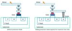
IC layouts go through extensive design rule checking to ensure correctness, before being accepted for fabrication at a foundry or IDM. There’s something called the antenna effect that happens during chip manufacturing where plasma-induced damage (PID) can lower the reliability of MOSFET devices. Layout designers run Design… Read More
Whether it is the stock market or the semiconductor market, the name of the game is yield. In semiconductors, yield has to do with minimizing scrap costs in all phases of manufacturing. This means squeezing as many good dies from a wafer as well as maximizing the number of good assembled/packaged chips that pass system level testing.… Read More
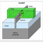
As transistor dimensions shrink to follow Moore’s Law, the functionality of the gate used to switch on or off the current is actually being degraded by the short channel effect (SCE) [1-5]. Moreover, the simultaneous reduction of voltage aggravates the degradation, as will be discussed below.
A Practical Lower Limit of… Read More
We live in an age of abundant information. There is a tremendous exchange of ideas crisscrossing the world enabling new innovative type of products to pop up daily. Therefore, in this era there is a greater need to understand competitive intelligence. Corporate companies today are interested in what other competitors are brewing… Read More
In my 40 years’ experience in power semiconductors I have visited thousands of customers, big and small, on every continent except Antarctica. When the issue invariably turns to the packaging of the power semiconductor – transistor, diode, or integrated circuit – the requests for improvement fall into six categories:
… Read More
In March 2010 Efficient Power Conversion (EPC) proudly launched our GaN technology at the CIPS conference in Nuremberg, Germany. Parts and development kits were readily available off-the shelf and therefore designers could immediately get started with a new state-of-the-art semiconductor technology.
… Read More
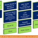
According to the IEEE Std 1012-2012, verification is the acknowledgement that a product is in satisfactory condition by meeting a set of rigorous criteria. [3] Transistor-level verification involves the use of custom libraries and design models to achieve ultimate performance, low power, or layout density. [2] Prediction… Read More
This post discusses attributes of gallium nitride (#GaN) that make it a disruptive technology and identifies the four factors required for GaN technology to displace silicon as the technology of choice.
Displacing the Silicon with GaN
38 years ago, when I first entered the semiconductor business as a freshly minted Stanford … Read More
In the semiconductor ecosystem, several partners (or better to say stakeholders) join together in the overall value chain to finally output the most coveted chip, err I should say SoC these days. It becomes really interesting when we start analyzing the real value added by each of them, none appears to be less. Well, then to whom … Read More