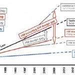
Over a decade ago, a group of semiconductor industry experts published a landmark paper as part of the periodic updates to the International Technology Roadmap for Semiconductors, or ITRS for short (link). The ITRS identified a critical design productivity gap. The circuit capacity afforded by the Moore’s Law pace of technology advancement was growing faster than the capabilities of EDA tools and flows to support the associated design complexity. The figure below captures the ITRS projections at that time.
Note that the ITRS experts recognized the increasing influence of design IP (and its reuse) to help mitigate the gap. Nevertheless, this ITRS report served as a ‘call to action’ for the EDA industry to address methods to improve design productivity.
Fast-forwarding a decade, how has the landscape changed? Moore’s Law has continued to enable tremendous growth in circuit density, a testament to the expertise and ingenuity of fabrication engineers and equipment manufacturers. Note that this process technology evolution has been achieved without a reduction in reticle size, truly an amazing achievement.
Many EDA tools have been re-architected (and design models optimized) in support of multi-threaded (and in some cases, distributed) computation for very large datasets.
EDA platforms have been introduced, integrating analysis algorithms into implementation flows to improve optimization decisions, and thus overall design closure schedules. In support of these timing, noise, and power optimizations, the design model (and cell library model) complexity has grown – this adds to the stress on dataset size.
I was curious to know, “How has the industry progressed in closing the productivity gap? What are the areas where the gap remains?”
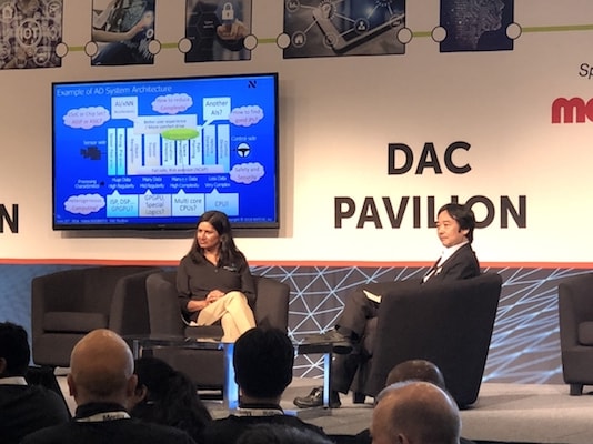
At the recent DAC55 in San Francisco, Cadence assembled a panel of industry and EDA experts to address the topic:
“Monster Chips – Scaling Digital Design Into the Next Decade”
The panel participants were:
- Chuck Alpert, Senior S/W Group Director for Genus Synthesis, Cadence
- Anthony Hill, Fellow and Director for Processor Technology, Texas Instruments
- Antony Sebastine, Principal Engineer with the Systems Group, ARM
- Anand Sethuraman, Senior Director, ASIC Products, Broadcom
- Patrick Sproule, Director of Hardware, P&R Methodology, Nvidia Corp.
Here are some of the insights the panel shared – both acknowledging the strides made in addressing the design productivity gap and highlighting remaining challenges.
Advances
“The growing use of (multiple instances of) hard IP has required significant focus on macro placement. Automated macro placement in design blocks has improved significantly – routing congestion is reduced.”
“DRC throughput – especially approaching tapeout – is always time-critical. The (distributed) physical design verification tools have kept runtimes in check.”
“The ECO-based flows to close on timing issues have improved substantially.”
“The signal buffering and advanced layer selection algorithms in GigaOpt provide better physical implementations—of course, pre-route to post-route correlation is always a challenge.”
Challenges
“Design implementation capacity must be improved. The Quality of Results (QoR) for blocks greater than 2 million instances tends to degrade substantially.”
“Agreed. We are constrained to block sizes of 1M-3M instances to achieve suitable turnaround time and QoR. The design partitioning overhead in floorplanning and constraint management is cumbersome. We need to be able to support block sizes of 20M-30M instances to keep pace with the technology.”
“We are utilizing physical design servers with 40 processors and 768GB to 1TB memory, but the (multi-threaded) jobs are still limited in throughput.”
“A flow of increasing importance is the calculation of dynamic P/G grid IR voltage drop, and the impact on timing margins. The tools need to have the capacity to support activity-based analysis on very large networks.”
Expanding upon the last comment, the significance of dynamic voltage drop (DvD) on design closure was a common theme throughout the DAC conference, both in technical presentations and the EDA vendor exhibit floor. Current SoC designs commonly incorporate several features that increase the sensitivity of timing analysis calculations with DvD-based characteristics:
- dynamic operation voltage domain optimization (DVFS)
- non-linear cell and interconnect delay dependence upon (reduced) P/G voltages
- (aggressive) library cell track allocation to the P/G rails
At advanced process nodes with aggressive voltage domain and power optimizations, static IR drop P/G analysis (with fixed cell characterization margins) will be increasingly problematic.
Summary
Chuck A. from Cadence offered a unique perspective to the comments from the other panel members. “Cadence wants to partner with design teams working on difficult blocks. We evaluate our implementation platform QoR on our internal testcases, but would benefit from a closer collaboration, to better understand the issues presented by specific designs.”
The takeaways from the discussion that I noted are:
Several EDA tool areas have made significant improvements in designer productivity and support larger dataset sizes – e.g., analysis-driven optimization algorithms, multi-threaded and distributed algorithms.
Nevertheless, designers are continuing to face the productivity gap identified a decade ago – support for block sizes of 20M-30M instances is required to keep pace with Moore’s Law. Specifically, physical design implementation flows require (academic and industry) research focus to be able to accommodate larger block sizes. Collaborative partnerships between (leading-edge) design teams and flow developers are required.
Patrick S. from TI reminded the audience that there will be an increasing demand to integrate reliability-based analysis algorithms into implementation platforms – e.g., EM, aging mechanisms. The goal would be to exit implementation and be ready for reliability sign-offmuch as EDA platforms strive for timing/noise signoff quality.
Alas, the EDA productivity gap is still present – a factor of 10X improvement in throughput is needed.
At DAC, I bumped into a professor colleague who lamented that EDA academic research funding was drying up, as there is a general perception that “all big EDA problems have been adequately addressed… the money is going to proposals associated with machine learning and AI.”In actuality, the challenges of efficient design data modeling, development of (tightly-correlated) optimization algorithms, and opportunities for improved (distributed) processing are more important than ever.
I guess you could consider this to be a 2018 version of the ITRS call to action.
-chipguy