webinar banner AI 2026 v2

SoC Design Partitioning to Save Time and Avoid Mistakes

SoC Design Partitioning to Save Time and Avoid Mistakes
by Daniel Payne on 12-18-2018 at 12:00 pm

I started designing ICs in 1978 and continued through 1986, and each chip used hierarchy and partitioning but our methodology was totally ad-hoc, and documented on paper, so it was time consuming to make revisions to the chip or train someone else on the history or our chip, let alone re-use any portion of our chips again. Those old, manual ways of doing chip designs are happily far behind us now, so much so that recent smart phone chips routinely have processors with billions of transistors, with massive amounts of semiconductor IP reuse, all enabled by more modern and automated IC design flows. This blog idea springs from information gleaned in a White Paper written by Methodics, a software company founded in 2006 with a headquarters in San Francisco. The big picture view at Methodics is to model your entire SoC as related sets of functional blocks, then automate the workflow to ensure that your chip design is consistent and easy to update and communicate changes and dependencies.

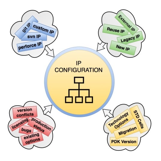
Here’s a picture of what they call an IP configuration and how it maintains multiple relationships to design data and versions:

The specific software tool at Methodics is called Percipient, and using this IP configuration approach you can do top-down designs more easily, because along the way the tool is tracking the content of each IP and the hierarchical relationship between them. These IP objects and relationships can be quickly captured at the very start of a project, even before the design details are ready. Everyone on the design team can visualize how their part of the project is being placed in a hierarchy and what its dependencies are going to be. Metadata is attached to each IP, so for example a Bluetooth IP block may require a specific PDK version from your foundry of choice and you can quickly determine if all IP blocks are compatible with that PDK version.

In the first diagram there’s a blue area showing that IP can be imported for re-use from many Data Management (DM) sources:

  • Perforce
  • git
  • Subversion
  • Custom

If your particular DM system isn’t listed, then just contact Methodics to see if they’ve already got an import available. The files in your DM can be primarily binary, text or a mixture of the two, so it’s your choice and there’s no restriction on DM type or how you make relationships between IPs of each type.

Workspaces are used to save specific configurations of your own choosing. Making changes to IP and its metadata can then be saved as a release, and each release has the relationships between all IPs in your hierarchy at that one point in time. With any particular release you can run simulation and functional verification, then the results are attached to that release. Everyone on your team can be notified when a new release happens on some IP.

There are even third party integrations with requirements management and bug-tracking tools, so team members always know for each IP what the requirements associated with it are, along with any bug reports. Here’e another diagram to show how an IP configuration connects with other tools in your IC flow:

So with the Percipient methodology you can go to one place and find out all information about your electronic system, from the top-level all the way down to the lowest block levels. You will know where each block is being used and how often it is being re-used, along with the requirements and performance, plus the history of changes made to it and by who. Searching through the Percipient catalog is quick and easy, so it takes a lot of the guesswork out of complex IC design projects.

Projects that need to comply with Functional Safety (FuSa) will enjoy the traceability features built-in to Percipient, so that you can validate every safety function automatically at each release. Another benefit to automating FuSa compliance is that user responses to questionnaires can be attached to specific IPs, and then managed throughout the design hierarchy.

OK, this sounds promising so far, but how do I know how to best partition my specific design with this tool? The best practice is to place anything that could be re-used into a functional block as its own IP object. A functional block can contain sub-blocks too, here’s another example of a hierarchy:

Your design team is typically comprised of groups, and each group can be responsible for their own releases. The best practice is to release early and often as progress is made and milestones are reached. Both producers and consumers of IP blocks use the Percipient tool, while a producer may be most interested in the latest version and a consumer could be more interested in using a fixed version that isn’t changing until they request an update. The producers are doing design work, running simulations and validations, reaching some quality goal and then they make a new release, alerting consumers that a new version is ready to consume. All team members are in the loop and quickly learn to choose the proper release.

Conclusion
Your SoC projects can be quite complex, containing Terabytes of data, so consider the benefits of using a proven, modern system to manage your IP with traceability, quickly and easily. Just look in one place to know the state of your design, while avoiding communication mistakes that could cost you an expensive silicon spin. The complete 7 page White Paper can be read here.

Related Blogs


Cadence Automotive Summit Sensor Enablement Highlights

Cadence Automotive Summit Sensor Enablement Highlights
by Camille Kokozaki on 12-18-2018 at 7:00 am

At the November 14 Cadence Automotive Summit, Ian Dennison, Senior Group Director, outlined sensor enablement technologies and SoC mixed-signal design solutions, from Virtuoso electrically aware design with high current, high reliability, yield and performance tools and methodologies enabling ADAS/AV sensors for vehicle perception.

An ADAS/AV camera system was described as containing on the transmit side a Cadence Ethernet MAC, a BroadR-Reach PHY, filters, cables, and connectors to a decision-making board on the receiving side and accompanying simulation-based EMI verification, modeling, PCB power integrity analysis, S-parameter models to ensure data coming in is successfully received without resending.

The actual IP containing the automotive Ethernet MAC IP is available in 10Mbps Ethernet that replaces CAN, Flexray, 100Mbps which still demands image compression, and a higher than 1Gbps rate that avoids the need for image compression for the highest image quality and best object classification, along with DMA, APB configuration interface registers and a time stamp unit for Time Sensitive Networking to ensure camera data is not delayed. The automotive Ethernet MAC has received ASIL-B ready certification under the Automotive ISO 26262 standard.

ASIL compliance requires a quality management process and certification, a safety manual for SEooC, safety features description, failure mode effect, diagnostic analysis, and automotive safety kits for tools and flows. In implementing a system using Innovus, a time stamp unit (TSU), the TSU block is duplicated with timer outputs compared on a cycle-by-cycle basis to detect any faults as one of the safety mechanisms. Other considerations exist like creating safety boundaries where internal nets are maintained inside each TSU and interfaces nets are not routed over to avoid common mode failures in the duplicated TSUs.

ISO 26262 SoC design compliance is ensured with the functional safety methodology described in the diagram. Some requirements for proper classification include continuous checks that are needed on the image sensor to enable failure signals to be raised within two frames. On-chip checkers are placed inside the chip to identify analog or digital functional failures that can result in image sensor row, column, ADC and clock failures. There are some types of image sensor failures that rely on DSP processes downstream to be properly detected.

There are some CIS ADAS/AV considerations that determine object classification success driven primarily by moving vehicle image quality. CIS ADAS/AV issues include high dynamic range (HDR) needed for bright/dark conditions, vehicle motion-induced rolling shutter distortion, LED street/vehicle lighting rolling shutter flicker mitigation needs, real-time shutter compensation, noise vulnerability, moving vehicle stabilization and gyroscope fusion and finally cost in a price sensitive automotive market.

A complete simulation platform for CIS analysis uses the ADE Product Suite and the Spectre family of simulators.

Designing needed CIS ADC high dynamic range includes considering the CIS fps/shutter speed that sets the ADC conversion rate, and CIS dynamic range sets the ADC resolution (60 dB and a range of 1000:1 means a 10-bit ADC). The Cadence methodology characterizes the ADCs in the presence of temporal noise.

Uniformity of the CIS arrays for proper design-in of electrical and electrical reliability is essential. Cadence Virtuoso electrically-aware design offers on-screen real-time parasitics and resistance analysis with colormaps and voltage drop summaries, and electromigration current flow, so they can be considered in the analysis and design.

Lidar uses several technologies such as CMOS used in SoCs for controller and Ethernet and image sensors, MEMS for scanning mirror, silicon photonics, III-V material for laser source, and system-in-package. The drive is towards low-cost, small form-factor lidar for automotive, medical, and industrial applications.

The end of Moore’s law is enabling a disaggregated SoC where packaging is the glue between different die where thermal integrity, AC coupling, losses, reflections, crosstalk, warping mitigation, thermal and electromagnetic integrity need to be comprehended and dealt with.

Silicon photonics for frequency modulated continuous wave (FMCW) requires 10 cm automotive lidar depth precision addressed with tighter control of laser modulation and an electro-optical phase-locked loop (PLL). A MEMs tunable laser producing a laser source is split down into two waveguides. One waveguide is sent to the target and the return signal is blended, using an FMCW with a frequency changing all the time and with the signature generating a beat frequency.

Silicon photonics and MEMS co-design are enabled with Spectre APS and AMS Designer, Virtuoso ADE, schematic and layout suites, along with tools from partners like Lumerical and Coventor.

Cadence’s Legato Reliability Solution has a design-for-reliability approach extending the lifetime of the chips. When a failure occurs, functional safety kicks in to stop a car, but tools are needed to help a design-for-reliability mindset where analog defect analysis occurs to reduce the test cost and eliminate test escapes, electro-thermal analysis prevents thermal overstress avoiding premature failures, and advanced aging analysis accurately predicts product wear-out.

In ADAS radar sensor design, antenna sizes are shrinking allowing on-chip integration. A 122GHz radar includes a low-noise amplifier (LNA), power amplifier, mixer, and two on-chip antennas.

The Virtuoso RF Solution allows multi-fabric RF in PCB, SiP and SoC and interfaces with Spectre RF, Allegro Sigrity and National Instruments’ Axiem. An ADAS radar transceiver design was illustrated showing stretchable transmission lines with pCells, matched RX & TX antennas, Spectre RF and Virtuoso ADE Assembler showing the noise figure, input matching, gain, and stability.

Virtuoso RF allows a layered extraction of modules with EM solvers using QRC (a parasitic extractor), Sigrity PowerSI (a 3D-EM solver), and NI’s Axiem (a 2.5D solver for planar elements). The Sigrity PowerSI 3D-EM has an RF-module package extraction and critical path S-parameter model extraction for layered structure designs (on-chip, package, and PCB).

Datacenters are well suited for labeling training datasets with a training engine run only once per dataset versus an inference engine that is run on every image from various sensors onboard the vehicle that feeds new data to the datacenter.

The labeling of the datasets generates a set of coefficients with various weights pushed to the car, which then does a single pass evaluation on the image and generates the most probable label for proper decision making.

System and software design follow a spectrum starting from workstation simulation with no specialized hardware, to Xcelium parallel simulation with hardware running at about 1KHz for software execution, moving to Palladium Z1 emulation with hardware running at ~1MHz for software execution, then to Protium S1 FPGA prototyping at ~10 MHz and finally with first silicon on a prototype board. This allows development of OS, middleware, firmware, and drivers in parallel with hardware-based simulation accelerating the functional verification. Early start to software development or the new hardware accelerate time-to-market.

The Cadence design enablement allows system and DSP design, advanced node SoC development, MEMS and Silicon photonics implementation, SiP integration and CNN software development, all in one interoperable environment that greatly enhances sensor design and opens design fabrics and opportunities leveraging improved accuracy, decision making, and reliability.

Read more here: Automotive Summit 2018 Proceedings


Photonics with CurvyCore

Photonics with CurvyCore
by Alex Tan on 12-17-2018 at 12:00 pm

As a preferred carrier to data or energy, photonics technology is becoming broad and diverse. In IC design, silicon-photonics technology has been the enabler of new capabilities and has revolutionized many applications as Moore’s-based scaling started to experience a slowdown. It acts as new on-chip inductor in HPC design and fast connectivity in network infrastructure.

At the Cadence Photonics Summit and Workshop 2018 held in San Jose last month, Cadence showcased its CurvyCore Infrastructure, a new technology intended for photonics applications. It is a native infrastructure in the Cadence Virtuoso custom IC design platform, allowing designers to create and edit complex curvilinear shapes common in photonics, RF, MEMs, microfluidics and conformal metal routing.

The State of Photonics Technology
The CurvyCore technology addresses markets and technologies that span from silicon photonics switches and interconnects for HPC/Datacenter, medical sensing applications, LiDAR, aerospace, MEMs to carbon nanotube conductors. According to Dr. Vladimir Stojanovic from UC Berkeley, who gave a keynote at the Cadence 2018 Photonic Summit, the current photonics integration with advanced electronics leverages CMOS transistor performance, its process fidelity and package integration, to enable emerging SoCs for various applications ranging from computing to sensing and imaging.

Based on his team’s research, the sweet spot for a “zero-change” silicon photonics platforms used in this monolithic integration technology is of either 45nm or 32nm SOI CMOS processes –they are suitable for adding photonic capability and enhancing integrated system applications such as main communication of computing tasks without involving complicated 3D integration efforts or double-patterning for EUV. Figure 1 captures the optical I/O landscape as well as the application of photonics on RISC-V microprocessor and DRAM.


Silicon photonics application for fast interconnects also evolved from a data center, off-chip centric type to be more integrated as on-chip feature in both microprocessor and PIM (Photonic-Interconnected DRAM) designs. The open-source RISC-V microprocessor with photonic on-chip interconnect was first implemented as single, electronics-optics hybrid chip, dual-core 1.65Ghz processor in CMOS 45nm SOI.

Challenges to Silicon Photonics
Embracing silicon photonics is an evolving process as handling curvilinear physical shapes is challenging. Unlike the traditional Manhattan polygons, custom design of curvilinear geometries is prone to misalignment, roundoff errors and manufacturing problems.
It is an effort intensive undertaking as its associated Pcell creation is cumbersome and time consuming. Additionally, a lack of common infrastructure leads to many ad-hoc, non-replicable and sub-optimal flows –translating to complex DRC/LVS problems to fix. All of these drives the need of having a robust platform to address the overall physical design automation.

CurvyCore Technology and Its Key Benefits
For an optimal performance, the CurvyCore technology has been natively implemented in the Virtuoso platform. The CurvyCore infrastructure has a three-tier data model and is an extension to the Virtuoso advanced-node platform, which sits on a high-performance symbolic mathematical engine.

As part of the Virtuoso expanded data-model, the CurvyCore infrastructure provides full access to all levels of design captures –from building block to actual symbolic expressions, enabling the creation and maintenance of differentiated curvy IP. For example, figure 3 shows phase shifters for a LiDAR (Light Detection And Ranging) application comprises of orthogonal polygons for the electrical connections and curvy geometries for optical interconnect –both of which can be concurrently viewed and manipulated.

The diagram in figure 4 illustrates the CurvyCore data model starting with the mathematical core which consists of an accurate mathematical representation thru symbolic equations, then is followed by the second layer (in magenta) that captures any curve geometries discretized to its equivalent shapes, and the top, physical layer (in pink), that contains the layout polygons in OA shapes. The combination of curvilinear discretization, boolean and sizing operations enables design rule fixing related to photonic complex shapes.

Aside from enabling the creation and editing of complex curvilinear shapes, the CurvyCore integration with the Cadence Virtuoso custom IC design platform leverages a unified design environment for the development of multi-fabric systems. It has new APIs to allow complex PCells creation and efficient data model to support high-performance editing or storage of curvilinear shapes within the Virtuoso design platform.

CurvyCore also supplements the Virtuoso Layout Suite and works seamlessly with the most advanced Virtuoso features, allowing true co-design and integration of electronics and curvilinear features. For example, during the Cadence Photonics workshop attendees were given the opportunity to use the Virtuoso custom IC design platform to view or edit a LiDAR photonics IC and to perform co-simulation of beam steering using Spectre® AMS Designer, MATLAB and Lumerical INTERCONNECT as part of a test-drive of the CurvyCore infrastructure implementation in the Virtuoso platform.

The CurvyCore technology is planned for general availability in Q1-2019.

For more about CurvyCore check HEREand for the Cadence 2018 Photonics Summit check HERE.


Intel Discontinues the Custom Foundry Business!

Intel Discontinues the Custom Foundry Business!
by Daniel Nenni on 12-17-2018 at 7:00 am

After mentioning what I heard at IEDM 2018, that Intel was officially closing the merchant foundry business as an aside in a SemiWiki forum discussion, I got a lot of email responses so let me clarify. Honestly I did not think it was a big surprise. Intel Custom Foundry was an ill conceived idea (my opinion) from the very start and was not successful by any measures. To be clear, it is not something I just heard, it is something I have verified through multiple sources so I believe it to be true, absolutely.

Just a little background, we started blogging about Intel in the early days of SemiWiki and have posted 202 Intel related blogs that as of today have been viewed 2,822,613 times which is an average of 13,973 per blog. Big numbers in the semiconductor blogging world in my experience. Intel has a very large group of entrenched supporters with even more naysayers that are not easily swayed so there are plenty of blog comments, some of which had to be deleted. My argument against Intel opening up their leading edge manufacturing facilities to the fabless community was that it would be a distraction from Intel’s core competency of making microprocessors. As we know, ecosystem is everything with the foundry business and that takes time, money, and technical intimacy, three things that Intel seemed to greatly underestimate.

Also read: Intel Custom Foundry Explained!

Altera was the big win for the Intel Custom Foundry business. I was having coffee with a friend in TSMC Fab 12 when it was announced. If my memory serves it was Dr. Morris Chang who made the announcement and it honestly felt like parents were divorcing. It was mentioned that TSMC viewed this as a learning experience and would make sure that losing an intimate partner like Altera would never happen again.

Also read: Apple will NEVER use Intel Custom Foundry!

Altera was founded in 1984, the same year I started my semiconductor career. Some of my school friends joined Altera and I worked with Altera as a customer during my EDA and IP career down to 20nm so I had a front row seat. It was a very close relationship between Altera and TSMC up until Xilinx came to TSMC at 28nm. TSMC gave Xilinx equal access which soured the Altera relationship. Altera then moved to Intel at 14nm which led to the acquisition at a premium price.

One of the funniest stories I heard was about the first copy of the Intel 14nm design rules Atera got from Intel. They were heavily redacted, which is something I had never seen in the foundry business. After many delays Intel put their own implementation team on the first 14nm Altera tapeout and the result was a very competitive FPGA chip. If not for the continued delays, Xilinx would have been in serious trouble as the Intel 14nm FPGA, based on my experience with customers, beats the Xilinx 16nm in both density and performance.

You can see the 2014 Intel Custom Foundry pitch HERE. Great intentions, good effort, too many broken promises, but doomed from the very beginning, my opinion.


Next-Generation Formal Verification

Next-Generation Formal Verification
by Daniel Nenni on 12-14-2018 at 12:00 pm

As SoC and IP designs continue to increase in complexity while schedules accelerate, verification teams are looking for methodologies to improve design confidence more quickly. Formal verification techniques provide one route to improved design confidence, and the increase in papers and interest at industry conferences like DVCon and DAC reflect the growing usage of formal verification tools in the industry. Despite the increase in usage of formal verification, there are still few opportunities for verification engineers interested in formal techniques to exchange ideas, knowledge, and best practices.

The Synopsys VC Formal Special Interest Group (SIG) events are a step towards broadening knowledge of formal verification. In the inaugural year of the VC Formal SIG, Synopsys held events in India, Japan, and the United States. In all three events, VC Formal customers shared their experience and successes in using VC Formal to address verification problems, alongside Synopsys AEs who presented new or advanced applications of formal verification. The most recent event was held in November in Santa Clara, California, with a keynote discussion from Sean Safarpour and Pratik Mahajan from Synopsys discussing the history and future of formal verification. The Santa Clara event showcased experts from AMD, ST Microelectronics, Qualcomm and Juniper Networks, highlighting the use of formal verification to solve challenging verification problems.

Formal Sign-Off of a Control Unit (AMD)
Wayne Yun discussed the verification of a complex control block using formal methods. The block included an AHB arbiter, microprocessor, data collector, accumulator, and glue logic. First, each block was considered in isolation. Formal techniques such as formal model creation, case splitting, invariant identification, and symbolic variables were applied to each sub-block. Assume-guarantee reasoning validated assertions on interfaces between sub-blocks. He also discussed how AMD used the coverage collection, overconstraint analysis, and fault injection features of VC Formal to signoff the design. VC Formal formal core analysis and fault injection identified several areas that required additional assertions. At the end of the project, over 94% of assertions were proven, all blocks had full formal core coverage, and most blocks detected over 99.8% of injected faults.


Formal Verification of a GPU Shader Sequencer (AMD)
Chirag Dhruv and Vaibhav Tendulkar showed the benefits of VC Formal FPV App’s bug hunting effort to find bugs in a GPU shader sequencer. A wide variety of parallel instructions, asynchronous events, and dynamic configuration changes make simulation coverage closure difficult in this block. Sub-block decomposition allowed quick bug exposure and rapid iteration time. Formal reachability analysis, COI coverage analysis, and formal core coverage analysis identified dead code and design areas requiring more assertions. Formal verification found over 30 RTL bugs, several which would have been difficult to discover through simulation, absolutely.

Accelerate Digital IP Formal Verification with Machine Learning Technology (ST Microelectronics)
Giovanni Auditore described a shift of verification resources within ST towards formal verification. They used Verdi Planner to combine the formal and simulation verification plans, allowing a single view of verification progress as formal use increased from project to project. A variety of VC Formal Apps were applied to the design, including FCA for unreachability analysis, FRV for register verification, and FPV for property and protocol verification. Giovanni also described how the Regression Mode Acceleration (RMA) feature of VC Formal sped up formal regression. RMA uses machine learning techniques to accelerate proof time on future runs of the same or incremental versions of RTL. After applying RMA learning to an initial release of RTL, proof time for subsequent RTL releases took 1/3 the time as running identical regressions without RMA. RMA also reduced runtime of fault injection qualification from 21 to 16.5 hours.

Verification Sign-Off with Formal (Qualcomm)
Anmol Sondhi shared how to layer various coverage metrics available in VC Formal to build confidence in assertion quality throughout the design cycle. Early in the project, cone-of-influence based property density will identify testing holes in the design. Unreachability analysis through the FCA App, and over constraint analysis identifies areas in the design where formal stimulus won’t reach, allowing targeted review of RTL and formal constraints. Formal core coverage represents the logic that formal engines use to prove a property. Uncovered areas represent potential test holes. Finally, fault injection identifies areas where modifications in RTL behavior trigger assertion failures. He also showed how RMA resulted in between 2X and 10X improvement in regression runtime. Using VC Formal, the example project achieved over 99.5% property density and 90% formal core coverage and identified only 12 areas of undetected faults that required further investigation.

Designing for Formal Verification (Juniper Networks)
Anamaya Sullerey explained how RTL designers can be involved with formal verification through design methodology and short, frequent formal regressions of RTL. He described how changing an event driven implementation with a complicated state machine and complex, interacting side effects to a functionally driven implementation with lots of small modules that perform simple tasks can simplify and accelerate formal verification. Efficient decomposition of the design allows for meaningful sub-block formal verification regressions of no more than five minutes. Other recommendations for formal friendly design include early parameterization of RTL code, isolating complex blocks into separate modules for easy abstraction, creating meaningful intermediate expressions, and coding assertions for design invariants such as one-hot bit vectors. With a high level of formal friendly design methods, designers or verification engineers could quickly build module level formal testbenches that catch a majority of bugs with five minutes of regression time.

The Synopsys formal verification team presented tutorials on datapath operations and how to discover design invariants. JT Longino talked about using Synopsys tools for formally proving datapath operations. Datapath correctness continues to be a challenge for the industry. High confidence in datapath operations is difficult or impossible to achieve using simulation, but datapath operations have historically exceeded the capacity of formal property verification tools. Synopsys HECTOR technology provides users the ability to prove equivalence between an implementation RTL design and a reference design. The two designs can have different latencies, and the reference design can be untimed C or C++ code. The new VC Formal DPV App integrated HECTOR technology into the VC Formal GUI, allowing formal verification engineers to work on datapath verification problems in a familiar environment.

Iain Singleton described how to use VC Formal to discover design invariants to help converge complex properties. Invariants describe properties that remain unchanged when a specific transformation is applied and can restrict the state space of subsequent proofs if used as assumptions. Although they are powerful tools or assisting convergence, invariants can be difficult to identify and write. The VC Formal Iterative Convergence Methodology (ICM) provides users a methodical, tool-assisted approach to identifying design invariants. Using ICM, convergence time for a selected set of difficult properties was reduced from over three hours to around one minute. To learn more about VC Formal and to stay up to date on dates on VC Formal SIG 2019 events, visit HERE.


Embeddable FPGA Fabric on TSMC 7nm

Embeddable FPGA Fabric on TSMC 7nm
by Tom Simon on 12-14-2018 at 7:00 am

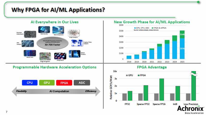
With their current line-up of embeddable and discrete FPGA products, Achronix has made a big impact on their markets. They started with their Speedster FPGA standard products, and then essentially created a brand-new market for embeddable FPGA IP cores. They have just announced a new generation of their Speedcore embeddable FPGA IP that targets leading edge compute applications such as AI/ML. More than just being a process node advancement, they have made a number of strategic architectural changes to improve performance and adapt to certain classes of problems.

Yes, as you might expect this announcement includes moving to the latest process node, TSMC 7nm, and there will be a back port to 16nm later in 2019. However, the really interesting stuff in this announcement has to do with further improvements in the already optimized architecture of the fabric.

I had a chance to speak to Robert Blake, Achronix CEO, at the time of the announcement to gain deeper insight into the specifics. He mentioned that they have successful 7nm validation silicon back that meets their target specifications. The motivation for many of the changes in this new generation are based on the AI/ML market and the big changes in how FPGA technology is being used.

FPGAs have made a dramatic shift over the decades from glue logic and interface uses to becoming a major element in data processing, such as networking and AI. Microsoft demonstrated how FPGAs offer huge acceleration for compute intensive applications. Classic CPUs have seen their year-to-year performance gains flatten out. With this there has been a concomitant growth of the use of specialized processors such as GPUs to fill the gap. FPGA’s represent an even more flexible tool for implementing computational processing. Achronix likes to point out that CPUs are rapidly becoming FPGA helpers, that can deal with exceptions, but are not necessarily in the main data path as much anymore.

The beauty of embeddable FPGA fabric IP is that significant overhead of an off-chip resource is avoided. These include off chip driver loads, board real estate, and interface speed limits.

The Speedcore 7t, which is built with their Gen4 architecture, provides significant PPA improvements. Robert told me that they see simultaneous gains in performance, power and area, namely a 60-300% boost in performance and a 50% decrease in power with an area decrease of 65%. Any one of these would be noteworthy, but they have a combined win. Robert walked me through some of the changes that contribute to these numbers.

Based on the needs of several important applications, Achronix has added or enhanced certain logic blocks. For instance, there is an 8-1 mux, which is critical for networking applications. Another is an 8-bit ALU that is heavily used for AI/ML. Robert also talked about their bus max function, dedicated shift registers, and LUT changes, all of which improve the compute power of their FPGA fabric.

Robert talked about numerous other additions, such as their programmable bus routing. This 4-to-1 bus routing capability can be cascaded to create wider busses. This will save LUT resources and offers a 2X performance improvement.

Going one step further, they have added a new compute block – a Machine Learning Processor (MLP). It is optimized for neural network (NN) matrix vector multiplication. It is clocked at 750 MHz and has flexibility in the number formats is can handle: Fixed point, Bfloat16, 16-bit half precision FP, 24-bit FP, block FP. The flexibility provided with varying configurations, allows customization to adapt to different NN algorithms. It also provides future proofing, because the programmable array can be altered as NN algorithmic technology advances.

There is so much in this announcement, I suggest referring to the Achronix website for all the details. However, it is clear that Achronix intends to maintain its technical and business advantage in this space using a wide range of targeted technical improvements. Rather than rest on their laurels, they are using their experience to help meet the emerging computational requirements for AI/ML, which is poised to become pervasive.


Sequential Equivalency Checks in HLS

Sequential Equivalency Checks in HLS
by Alex Tan on 12-13-2018 at 12:00 pm

Higher level synthesis (HLS) of an IP block involves taking its high-level design specification –usually captured in SystemC or C++, synthesizes and generates its RTL equivalent. HLS provides a faster convergence path to design code stability, promotes design reuse and lowers front-end design inception cost.

HLS and Mentor Catapult Platform
The current rise in the HLS adoption has been partly attributed to the availability of verification solutions, which facilitate the validation of the generated RTL codes against the high-level reference design. Both design abstractions can be validated through either simulation based verification (such as coverage metric and assertion driven), or formal verification method to check for their equivalencies.

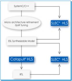
Mentor’s Catapult® HLS Platform provides a complete C++/SystemC verification solution that interfaces with Questa® (or third party simulators) for RTL verification as shown in figure 1. The platform consists of a design checker (Catapult DesignChecks or CDesign Checker), a coverage tool (Catapult Code Coverage or CCOV), a high-level synthesis (Catapult HLS) and a formal tool SLEC HLS (Sequential Logic Equivalence Check).

Logic and Sequential Transformations
During RTL-GDS2 design implementation, timing optimization frequently necessitates logic restructuring and transformation to meet PPA (Power Performance Area) tradeoffs. While critical timing paths can be resolved through the manipulation of logic cone topology –such as buffering, drive strength adjustments, better resource sharing, and an interconnect layer promotion, sequential related design manipulation can provide opportunities for solving critical timing paths that otherwise impossible to tackle. Such design transformation is hardly available in the later stage of gate level timing optimization as it may introduce state changes and complicates the verification tasks.

Several timing driven sequential modifications include pipelining (managing number of stages along data or control paths to meet throughput target); register retiming (shifting register to balance logic cone latency); state recoding in FSM block (such as from binary-encoded to one-hot implementation); and resource scheduling (what-if scenarios to meet optimal area and performance targets).

Furthermore, a number of design refinements might also introduce changes in sequential element count such as a block interface conversion from abstract data types to bit-accurate busses and augmenting test mode operation involving scan path logic insertion.

Designer also run Catapult HLS to generate power optimized verification ready RTL, which involves sequential transformations due to enable manipulation technique (enable extraction or strengthening) –yielding further clock gating that reduces switching activities. Figure 2 shows the additional clock gatings due to sequential analysis.

All of the previously described design changes alter the maps between registers of the two design abstractions, and render traditional combinational equivalence checkers ineffective. Instead, designers could run SLEC HLS to validate between C++/System C to RTL as well as RTL versus RTL (before and after an incremental power optimization).

The Mechanics of SLEC HLS
Unlike the traditional equivalence checker for combinational logic, proving equivalency across two design abstraction such as C++ versus RTL requires a different approach such as identifying the sequential differences. SLEC HLS has advanced analysis that allows designers to explore what-if refinements that normally might trigger traditional equivalence checkers to generate a false positive. It employs a fine-grain partitioning of design sections in order to provide scalability in handling large design codes.

As illustrated in figure 3, fracturing a function to its associated basic blocks, SLEC HLS analyzes and map them to its corresponding control FSM to schedule the dataflow analysis. Comparison is then performed at the interface of these “state-like” basic blocks along the time axis using micro transactions. HLS synthesis provides both basic block boundaries and information about the micro transactions.

Running and Analyzing SLEC HLS Results
SLEC HLS run setup is quite straight-forward and is achieved by black-boxing non-synthesizable design parts including large memory blocks, and specifying the same reset states and sequences usually captured for synthesis. Other design setting such as state correspondence, which reduces verification complexity as well as clocking and port mapping are automatically derived from the high-level reference codes. To improve run time and quality of results, the tool uses function-based partitioned blocks in the form called CCOREs (Catapult C Optimized Reusable Entities) –which are called for multiple times in the design, to perform a hierarchical verification.

At SLEC HLS run completion, there are 3 possible outcomes: a full proof of equivalency, a mismatch, or a partial proof –which indicates that some remaining points in logic being compared needed further analysis. A neat feature of SLEC HLS is when a mismatch occurs. In this instance, it will generate counter example testbenches containing stimulus sequences that designers use to trace design differences. These testbenches include flip-flop initialization values and all primary input stimuli intended to demonstrate the difference –which are simulation ready, and can be used for further analysis with functional verification tool. Subsequent fixes to mismatches may involve source code or I/O cycle/sampling adjustments, constraint changes and a rerun.

In the case of a partial proof, SLEC HLS will generate a formal coverage report that quantifies the exploration of all possible inputs and states, which is helpful to root-cause issues such as dead-code situation. Such information can also be used to identify incorrect assumptions or constraints that were provided to SLEC HLS such as conflicting dual assignments to an input. Hence, adding a formal verification in the flow reduces the need to do full-blown RTL simulation and cutting the overall verification time.

As part of the Catapult HLS Platform integrated verification solution, SLEC HLS provides designers with formal validation of designs across different abstractions (C++, SystemC, RTL) or refinement stages (pre- vs post-power optimization). Such vectorless validation can be used to complement simulations to deliver a more comprehensive verification and reducing the overall efforts and cost.

Check HERE for HLS and HERE for SLEC HLS.


Big Data Analytics in Early Power Planning

Big Data Analytics in Early Power Planning
by Bernard Murphy on 12-13-2018 at 7:00 am

ANSYS recently hosted a webinar talking about how they used the big-data analytics available in RedHawk-SC to do early power grid planning with static analytics, providing better coverage than would have been possible through pure simulation-based approaches. The paradox here is that late-stage analysis of voltage drops in the power distribution network (PDN), when you can do accurate analysis, may highlight violations which you have no time left to fix. But if you want to start early, say at floorplanning where you can allow time to adjust for problems, you don’t have enough information about cell placement (and therefore possible current draw) to do accurate analysis.

ANSYS have a solution based on something they call Build Quality Metrics (BQM). In the webinar they talk about the general methodology. There are multiple ways to approach BQM; one starts with a static analysis of the design (no simulation) and doesn’t require placement info. For this you build heatmaps based on simultaneous switching (SS) calculations, likely issues in the planned power grid and likely timing criticality. For SS, you calculate peak current per cell based on library parameters and operating voltage. You then combine these values for nearby instances which have overlapping timing windows (taken from STA analysis), summing these currents to generate an SS heatmap.

Next you want to look at where you may have excessive IR drop in the planned grid. In BQM, since you don’t yet have cell instance placements you fake it by placing constant current sources at a regular pitch on the low metal segments and then do a static solve to generate an IR-drop heatmap. The evenly-spaced current draw won’t match exact cell instance current draws but it should be a reasonable proxy, allowing these heatmaps to be generated early in implementation and refined as placement data becomes available.

You can further refine this analysis using timing slack data generated from STA analysis data to prioritize timing critical cases. Combining all these heatmaps together generates the ultimate BQM heatmaps. ANSYS and their customers have shown that there is excellent correlation in observed hotspots between these and heatmaps generated through the traditional RedHawk (non-SC) path.

All of this analysis leverages the ANSYS Seascape architecture underlying RedHawk-SC to elastically distribute compute to build heatmaps. Which means that analysis can run really quickly, allowing for an iterative flow through block place and route. Which is really the whole point of the exercise. Instead of building a PDN based on early crude analyses like shortest path resistance checks, then doing detailed analysis on the finished PnR to find where you missed problems with real vectors, the BQM approach provides high coverage earlier in the flow, without need for vectors or cell placement, enabling incremental refinement to the PDN as you approach final PnR.

ANSYS reports that runtime of the BQM approach can be 3X faster than a dynamic analysis based on just a single vector. Note that the static approach in BQM provides essentially complete instance coverage (all instances are effectively toggled) whereas dynamic coverage is inevitably lower. You can raise dynamic coverage by adding more vectors but then runtime becomes even higher. Overall, you can build and refine your PDN early, avoiding late-stage surprises, you can do this quickly enough that it makes sense as an iterative step in the PnR flow. You’ll still do signoff at the end with whatever method you feel comfortable. Just without nasty surprises. What’s not to like?

ANSYS tells me they have scripts to automatically setup the SC flow from your RedHawk setup, so it seem like there’s really no excuse not to give this a whirl 🙂 You can register to watch the webinar HERE.


DVCon is coming in February, now is the time to register early

DVCon is coming in February, now is the time to register early
by Daniel Payne on 12-12-2018 at 7:00 am

As 2018 wraps up this month it’s time to start thinking and planning for 2019, and if you work in the Silicon Valley then you’ll want to consider adding the 31st annual DVCon event planned for February 25-28 in San Jose. Surveys have shown for some time now that verification tasks actually take up more time on a SoC project than design does, so it makes sense to find out what’s new for verification engineers through:

  • 39 Technical papers
  • 25 Poster sessions
  • Two Panel discussions
  • Four Tutorials
  • Eight Short workshops


The Accellera Systems Initiative is the sponsor for DVCon, and they grind out the much needed standards so that our industry doesn’t get polarized by proprietary and conflicting software automation approaches.


The Universal Verification Methodology (UVM) can track its history from the Open Verification Methodology (OVM) and even the e Reuse Methodology (eRM) from Verisity back in 2001. Cliff Cummings leads a tutorial on Monday, February 25th all about UVM:

  • “Gain Valuable Insight into the Changes and Features that are Part of the New IEEE 1800.2 Standard for UVM and How to Mae the Most of Them”

Cliff Cummings is President of Sunburst Design, Inc., a company that specializes in world class Verilog, SystemVerilog, UVM Verification and synthesis training. Mr. Cummings is an independent consultant and trainer with 33 years of ASIC, FPGA and system design experience and 23 years of Verilog, SystemVerilog, synthesis and methodology training experience. Mr. Cummings has completed many ASIC designs, FPGA designs and system simulation projects, and is capable of answering the very technical questions asked by experienced design engineers.

For keynote this year you’ll hear about the topic of the “Thriving in the Age of Digitalization” from Fram Akiki, VP Electronics & Semiconductor Industry for Siemens PLM Software. Fram’s background includes 21 years at IBM spanning roles in analog IC design, microprocessor manager and GM. His next 13 years were at Qualcomm as a director of operations, then head of the mobile computing connected products.

There’s a buzz around all things RISC-V, so check out the panel discussion on Wednesday, February 27th entitled, “Verification and Compliance in the era of open ISA- is the Industry ready to Address the Coming Tsunami of Innovation?“. Moderator Mike Demler is a Senior Analyst at The Linley Group, and the panelists include:

  • Emerson Hsiao, Andes Technology
  • Adnan Hamid, Breker Verification Systems, Inc.
  • Rob Shearer, Facebook
  • Simon Davidmann, Imperas Software Ltd.
  • Neil Johnson, XtremeEDA Corp.

Neil Johnson is active on Twitter and his tweets are focused on functional verification.

Networking throughout the conference is available during the Expo on Monday from 5PM to 7PM, then again on Tuesday and Wednesday from 2:30PM to 6PM. View the complete agenda online here, and register online now to get the best prices.

DVCon is the premier conference for discussion of the functional design and verification of electronic systems. DVCon is sponsored by Accellera Systems Initiative, an independent, not-for-profit organization dedicated to creating design and verification standards required by systems, semiconductor, intellectual property (IP) and electronic design automation (EDA) companies. In response to global interest, in addition to DVCon U.S., Accellera also sponsors events in China, Europe and India. For more information about Accellera, please visit www.accellera.org. For more information about DVCon U.S., please visit www.dvcon.org. Follow DVCon on Facebook https://www.facebook.com/DvCon or @dvcon_us on Twitter or to comment, please use #dvcon_us.


56G and 112G SerDes Where the rubber meets the road

56G and 112G SerDes Where the rubber meets the road
by Tom Simon on 12-11-2018 at 12:00 pm

No matter how high the processing capability of a chip, its overall performance is limited by IO speed. This is very similar to a car with low performance tires, a powerful engine will not be able to transfer its energy to the ground effectively. There is quite literally a race going on between core processing and IO speeds for transferring data on and off of chips. AI, autonomous vehicles, 5G and other advances are pushing a never-ending drive to increase data transfer rates.

One interesting area of innovation is in cell towers, where the radios used to sit in a box on the ground and high power RF signals were carried over copper to the antennas. This architecture created power and cooling problems among others. Common Public Radio Interface (CPRI) uses optical cables to carry the digitized RF signal to an RF power amplifier on the cell tower mast. Interestingly when this happened, carriers realized that they could architect their fronthaul to move the Base Band Units (BBUs) to or near the central office. The BBUs rely on high speed data links to get their job done.

Another area of innovation is the advent of Top Rack (TOR) switching. While it shortened the distance from server blades to the data switches, it also comes with a huge upward demand in transfer rates. The pivotal player in all these and many other changes in data transmission paradigms is the ubiquitous SerDes. Big changes have been needed to move from 28G to 56G and 112G and at the same time to limit cross talk and noise as the number of lanes increases.

High speed SerDes are needed not just for short reach connections, the demand for longer lines adds more consideration in SerDes Design. Other requirements for SerDes are back compatibility for lower data rates andlegacy protocols, and the ability to support copper and fiber. eSilicon, a leading provider of complex FinFET ASICs, has put out an interesting article discussing the complexities of designing SerDes for the leading-edge ASICs they deliver. This is in part due to their presence in the networking, AI and 5G markets as silicon a provider.

In their article, they touch on the need to move to PAM4 from the older PAM2/NRZ operation. Multiple bit-levels add complexity, with level detection made more difficult due to switching levels closer to threshold voltages. The leading edge SerDes, operating at 56G and 112G, are both digital and analog, making their design a challenging prospect.

eSilicon also talks about the increased need for on-chip testing and verification features. They have added full speed digital and analog loopback, and also a variety of smart monitoring features. With all this said, eSilicon has 7nm SerDes that are proven in silicon.

Innovation is needed to keep up with the demands for moving data. Ethernet is moving from 100GbE to 400GbE. The data rates for CPRI, mentioned above, are pushing upward from 25Gb/s to 50Gb/s. Back planes and data centers are soon going to be running at 25.6 and 51.2 Tb/s. More data sources, more data consumers, faster networks and high volumes of video and audio real-time data are all pushing technology forward. The eSilicon paper on 56G and 112G SerDes is pretty interesting and worth reading through to get an idea of what is needed to make fast chips move data effectively.