webinar banner AI 2026 v2

You Will Not Get Fired for Choosing RISC-V

You Will Not Get Fired for Choosing RISC-V
by Camille Kokozaki on 12-27-2018 at 7:00 am

These were the closing words Yunsup Lee, CTO, SiFive used at one of the December RISC-V Summit Keynotes entitled ‘Opportunities and Challenges of Building Silicon in the Cloud’. Fired up was more the mood among the 1000+ attendees of the RISC-V Summit held at the Santa Clara Convention Center and SiFive was among the companies showcasing their latest offerings, providing an update among the increasingly active and productive ecosystem blending open-source initiatives with commercial products and services.[1]

Among the stats presented by Lee was the number of industry RISC-V cores released which will soon reach (in less than five years) more than 70 cores. 5,000+ registered to attend the SiFive Global City Tours and 500+ fabless semiconductor companies have contacted SiFive.

SiFive’s Core IP comprises the 2, 3, 5, and 7 Series. Each numbered series is a product family and comprises 32 and 64-bit offerings in E, S, and U variants. E cores are 32 bit embedded cores, S cores are 64-bit high performance embedded cores, and U cores are Linux-capable. Each Core IP Series comprises standard cores as well as cores that can be fully customized with the features of each available Core IP Series.

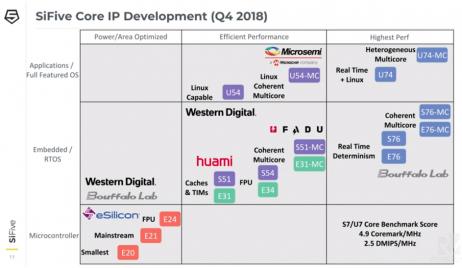
SiFive’s Core IP portfolio has rapidly expanded of late. In February 2018, the E2 cores of the 2 Series Core IP were launched. These are SiFive’s most efficient cores optimized for power and area. At the recent Linley conference, six cores were announced (E7, S7, U7, and their multicore versions) including the highest performance S76 and E76 cores with real-time determinism, the S76-MC, and E76-MC coherent multicores, the U74 real-time + Linux, and the U74-MC Heterogenous Multicore (used by Bouffalo Lab). The S7/U7 Core benchmarks clock at 4.9 Coremark/MHz and 2.5 DMIPS/MHz

Announced standard cores to date include the E20, E21, E24, E31, E34, S51, S54, U54, and U54-MC. Recent customizable Core IP design wins include eSilicon, Bouffalo Labs and Western Digital. The E31 has been implemented by Huami. SiFive also announced floating point features in numerous cores including the S54 and E34. The Linux-capable, coherent multicore U54-MC is used by Microsemi, a Microchip company while FADU has selected S51-MC and E31-MC coherent multicores with FPUs.


[1] The RISC-V Foundation Summit had about 1,200 registrations, with 32 countries and 23 states represented at the Summit, 29 exhibitors, 9 keynotes, 4 panels, 53 presentations, and 1 hackathon
The SiFive Embedded Software Ecosystem is growing, complementing SiFive Freedom Studio with offerings and compatible services from SEGGER, Lauterbach, IAR, Ashling, Imperas, UltraSOC with Embedded OSes like Express Logic-ThreadX, FreeRTOS, Zephyr, Micrium uCOS, RIOT, RTEMS, NuttX.

SiFive is building products to allow customization at scale with their online design platform with a web interface, allowing for the generation of customized RTL with their Core Designer. Eventually, Core Designer designs will be able to put into the Subsystem Designer to build RTL ready subsystems which can then be integrated with the Chip Designer (currently in development stage) to generate a chip for prototyping and silicon production readiness. Currently, only a web preview of the Chip Designer is available; an SoC template incorporates DesignShare IP from 3[SUP]rd[/SUP] part vendors (currently numbering 20), SiFive IP, and custom IP. All this is done through a cloud infrastructure (Microsoft Azure), in conjunction with an EDA tools company (Cadence) with SiFive offering the front-end Design Layer platform and managing the back-end Fab and OSAT packaging and test relationships. The proof of concept SoC was taped out in September (see below).

A variant of the FU540 was taped out in 28nm to prove the methodology. The variant was the first to utilize the combined cloud environment of TSMC’s VDE (Virtual Design Environment, announced at TSMC’s last OIP event), with Cadence tools, hosted on Microsoft Azure, with a SiFive’s web-based design integration and aggregation.

When asked what the biggest impediment to faster RISC-V adoption was, Yunsup Lee cited FUD (Fear, Uncertainty, Doubt) concerns and questions on whether the ecosystem is mature enough. He stressed that RISC-V is here and with everyone’s help working on RISC-V, it will be even stronger.

Yunsup Lee earlier had another presentation with Frans Sijstermans of NVIDIA where he described SiFive’s Freedom Unleashed Platform running NVIDIA’s open-source Deep Learning Accelerator (NVDLA) targeted toward edge devices and IoT. I had a chance to chat with him about this and he described a demo using a RISC-V Linux processor talking to NVDLA and running YOLO (You Only Look Once) v3 open source network. All components to test that out are open sourced and the code can be downloaded by anyone.

Summit announcements included Microsemi’s PolarFire SoC architecture which brings real-time deterministic asymmetric multiprocessing (AMP) capability to Linux platforms in a multi-core coherent central processing unit (CPU) cluster. This architecture, developed in collaboration with SiFive, features a flexible 2 MB L2 memory subsystem that can be configured as a cache, scratchpad or direct access memory. A PolarFire SoC development kit is also available, consisting of the PolarFire FPGA-enabled HiFive Unleashed Expansion Board and SiFive’s HiFive Unleashed Development Board with its RISC-V microprocessor subsystem and NVIDIA’s NVDLA was onboarded among a flurry of announcements.

Lee mentioned that SiFive’s strategy to build the HiFive Unleashed development board and getting the software stack going is helping the security aspects and all the software being ported is great to see and is helping the ecosystem. The next steps for SiFive are to increase adoption with some people who are still on the sidelines by highlighting the successes. For example, FADU in Korea announced that they used the S5 series as a real product reporting 1/3 of the area and 1/3 of the power required had they used standard cores. In addition, standard cores had features that they did not need. SiFive gave them a tailored implementation.

Software and hardware are important, and people want the easiest way to solve their problems. People are seeing the benefits of this approach since they cannot build only one chip due to the requirements being diverse. According to Lee, SiFive is building what customers want who are now asking for high- performance templates with HBM, Interlaken, high-speed Ethernet, high-speed SerDes. SiFive is getting a lot of pull on AI/ML and automotive safety requirements, edge compute, industrial solutions whose needs are not currently being satisfied. More custom solutions will be needed, and customers will see that standard products do not meet their needs and a customizable and configurable Design Platform will be the way to go. In summary, Yunsup Lee came to the Summit to deliver one message: RISC-V is here. RISC-V is safe. RISC-V is better. You will not get fired for choosing RISC-V.


[1] The RISC-V Foundation Summit had about 1,200 registrations, with 32 countries and 23 states represented at the Summit, 29 exhibitors, 9 keynotes, 4 panels, 53 presentations, and 1 hackathon


Physical Verification with IC Validator

Physical Verification with IC Validator
by Alex Tan on 12-26-2018 at 7:00 am

If a picture worths a thousand words, a tapeout quality SoC design with billions of polygons would compose a good book. To proofread this final design transformation format requires a foundry driven DRC/LVS signoff solution that nowadays is becoming more complex with further process scaling and shrinking pitch dimension.

Despite being frequently considered as the long pole in the tapeout cycle, physical verification step provides the needed critical assurance to a silicon success. As a leader in the physical verification (PV) domain, Synopsys IC Validator provides a comprehensive DRC/LVS signoff solution that delivers shorter time-to-results while supporting scalability, ease-of-use and ample runset coverage across various process nodes.

Tool Integration
Depending on its application context, IC Validator can be used in conjunction with different adjoining tools. For example in the custom design environment, it is integrated through Extraction Fusion and DRC Fusion –as part of the Synopsys Custom Design Platform along with other design and verification tools such as HSPICE, FineSim, CustomSim for circuit and reliability analysis, Custom Compiler and StarRC parasitic extraction. The intent of such tight integration is to accelerate custom and AMS design development. The Custom Design Platform is based on the popular OA (OpenAccess) database. It includes a complete set of open APIs for third-party tool integration as well as Tcl and Python programming support.

On the other hand, IC Validator also complements the Fusion Design Platform as a signoff element. Its seamless integration with IC Compiler II place and route system has enabled designers to perform independent signoff-quality analysis and automatic repair within ICC II –a process known as In-Design physical verification.

Customer shared challenges and experiences
In general, we could categorize three major selection criteria for a good physical verification solution, namely: total turnaround time, capacity and coverage support to foundry driven DRC/ERC analysis or fixing.

As an IC Validator adopter, IBM has utilized IC Validator Explorer –a DRC feature, to perform about a thousand basic checks in the shortest time possible. The check took 5 hours using only 8 processors, a much shorter verification compared with its corresponding full-chip DRC job involving 15.7K checks plus 160 processors and hours of runtime. Such precursor, stand-alone IC Validator Explorer run was done to evaluate design data integrity without the potential risk of hitting an incomplete job due to unintended, injected setup or basic errors such as misplaced units, P/G shorts, incorrect library. Only after a successful completion of such initial run, a full DRC is kicked off.

With respect to scalability, IC Validator turnaround time has also been proven to be quite linear. Another customer, SocioNext had confirmed scalability performance of 2.95x with 3x CPUs.

Metal Fill and DRC Related Fixes
In order to satisfy foundry requirement –which relates to retaining uniformity in metal density post CMP, metal fill has become a key element in tapeout preparation. There are two mainstream approaches, a shape based foundry fill and track based metal fill. Failure to apply proper metal fill may translate to an adverse timing impact depending on the inclusion or exclusion of the adjacent layer of the fill to the capacitance (which could shift by 10% or more).

Track based metal fill tends to deliver higher density while not requiring a runset as in the case of foundry based fill (instead, it is a techfile based). Additionally, the timing aware, color balanced track based fill generates a better yield, since regular shapes makes lithography patterning more consistent. Designers have finer and tighter density control, such as layer-by-layer control and defining window size target per layer. The density controlled is intended to balance DFM design rules and timing.

Using IC Validator with In-Design Technology allows an incremental and automated fill post ECOs. The tool identifies and performs fill on changed areas or layers. It is fast and natively done in NDM, requiring no streaming or tool setup. Fill removal around timing critical nets also preserves timing.

As the types of DRC related analysis and fixing are increasingly diverse, there are more acronyms and terminologies introduced over the course of few process nodes rollout –including the following terms:

  • ADR (Automatic DRC Repair), in which Synopsys Zroute is called to fix the DRCs and minimal impact to route topology or timing changes;
  • PERC (Programmable Electrical Rule Check), a feature in IC Validator that enables designers to validate new class of mixed-mode checks by combining netlist checks with geometric checks;
  • PM (Pattern Matching), a rule-based signoff feature for pattern-driven verification. It enables quick identification and perform subsequent automatic correction of potential manufacturability hotspots in a design by comparing them against a library of known problematic layout patterns.

IC Validator Landing Page
The examples discussed above represent some snapshots of how designers could tap IC Validators functionalities. To further facilitate such a growing list, Synopsys PV team has created a media collage of IC Validator related to flow customization, customer experiences and quick tips and how-to here. The collection is comprised of short videos of few minutes to no more than 5 minutes long.


Ethernet Enhancements Enable Efficiencies

Ethernet Enhancements Enable Efficiencies
by Tom Simon on 12-25-2018 at 7:00 am

Up until 2016, provisioning Ethernet networks was a little bit like buying hot dogs and hot dog buns, in that you could not always match up the quantities to get the most efficient configuration. That dramatically changed when the specification for Ethernet FlexE was adopted by the Optical Internetworking Forum as OIF-FLEXE-01.0. The surging demand for higher data rates and more flexible network configuration led to this innovative addition to the Ethernet standard.

FlexE fits in between the MAC and PHY, using MII interface signals. In fact, its operation can be so transparent that it is called a FlexE shim and can be completely transparent to existing physical transport layers. Of course, there is a FlexE ‘aware’ configuration that offers further flexibility for transport hardware that is aware of FlexE.

There are three main operations that FlexE can perform. Using these, a number of significant networking efficiency problems can be solved. The first is bonding, where large data pipes can be connected to multiple lower bandwidth physical lanes. For instance, five 100 GE lanes could be used to support a 500Gbps connection. FlexE can do this without the ~30% loss of efficiency of the link aggregation (LAG) solutions previously used for this purpose. Also, FlexE makes the connection performance deterministic, another advantage over LAG.

The second main capability of FlexE is sub-rating of links. There are instances where a link may operate more efficiently at a lower bandwidth than its interface rating. One example provided by the OIF is where a 300 Gbps link is desired, but its coherent optical physical layer needs four 75 Gbps inputs to send 150 Gbps each over two wavelengths. OIF points out that FlexE allows four 100 GE lanes to carry only 75 Gbps each to suit these needs. The down conversion from 300 Gbps is done in the FlexE shim that feeds the four 100 GE lanes.

The Third major feature of FlexE is channelization, where multiple data streams can be intermixed on one or more FlexE links. This is convenient for cases like 5G where there will be a number of smaller streams that can be interleaved into larger links and be recovered at the endpoint. This delivers a mechanism that allows service providers to offer deterministic Ethernet-oriented pipes of flexible width.

Anyone designing silicon that uses Ethernet will want to incorporate FlexE functionality to ensure optimal and full use of physical layer transport. Along with FlexE, another essential IP for chips that perform communications and networking is forward error correction (FEC). The move to PAM4 with multilevel signaling is exacerbating this need because the higher bandwidth it offers comes with a penalty in the signal to noise ratio, leading to higher bit error rates (BER).

Fortunately, Open-Silicon (a SiFive Company), a leading SOC development solution provider, offers IP that enables their customers to build high performance SOCs that take full advantage of high bandwidth Ethernet, FlexE and FEC for PAM4. The three components of this are Ethernet PCS IP, FlexE IP and multi-channel/multi-rate FEC IP.

The PCS IP supports 64b/66b encoding and decoding and is compatible with a wide range of MII versions. It runs from 10G to 400G. As mentioned above the Open-Silicon FlexE IP supports FlexE aware and unaware interfaces. Their FEC can be used in SerDes that support PAM4 and run up to 400G and can connect up to 32 SerDes lanes. It also can be used for Interlaken as well as Ethernet.

With high speed and high efficiency date transport continuing to be an essential prerequisite for business success, solution providers need to have networking solutions that allow facile data flow from the edge to the cloud to support increasingly complex business models and end-user functionality. Open-Silicon is continuing to maintain a technological edge in this area with the addition of this set of communications related IP.


Slowing growth in 2019 for GDP and semiconductors

Slowing growth in 2019 for GDP and semiconductors
by Bill Jewell on 12-24-2018 at 7:00 am

Growth in the global economy is expected to slow in 2019 from 2018. Ten economic forecasts released in the last two months show the percentage point change in World GDP from 2018 to 2019 ranging from minus 0.1 points to minus 0.4 points.

[table] border=”1″ cellspacing=”0″ cellpadding=”0″ align=”center”
|-
| colspan=”2″ style=”width: 521px; height: 23px” | Percentage Point Change in World GDP Growth, 2018 to 2019
|-
| style=”width: 98px; height: 19px” | Change
| style=”width: 423px; height: 19px” | Sources
|-
| style=”width: 98px; height: 19px” | -0.1
| style=”width: 423px; height: 19px” | Conference Board
|-
| style=”width: 98px; height: 19px” | -0.2
| style=”width: 423px; height: 19px” | The Economist, OECD, Oxford Economics
|-
| style=”width: 98px; height: 19px” | -0.3
| style=”width: 423px; height: 19px” | Pimco, Goldman Sachs, Euromonitor, Atradius, TD Economics
|-
| style=”width: 98px; height: 19px” | -0.4
| style=”width: 423px; height: 19px” | Schroders
|-

The major contributors the slowing growth are the two largest economies – the United States and China. Together these two countries account for about 39% of world GDP, according to the IMF. Euromonitor forecasts a half point deceleration in GDP growth for both the U.S. and China from 2018 to 2019. Euromonitor cites trade tension between the U.S. and China as a major factor in the slowing growth of each economy. Other factors are a maturing of the U.S. business cycle and the continuing slowing growth of China.

[table] border=”1″ cellspacing=”0″ cellpadding=”0″ align=”center”
|-
| colspan=”4″ style=”width: 594px” | Percentage Point Change in World GDP Growth, 2018 to 2019
|-
| colspan=”4″ style=”width: 594px” | Source: Euromonitor, December 2018
|-
| style=”width: 102px” |
| style=”width: 150px” | GDP Growth
| style=”width: 162px” | GDP Growth
| style=”width: 180px” | Point Change
|-
| style=”width: 102px” |
| style=”width: 150px” | 2018
| style=”width: 162px” | 2019
| style=”width: 180px” | 2018-2019
|-
| style=”width: 102px” | World
| style=”width: 150px” | 3.8
| style=”width: 162px” | 3.5
| style=”width: 180px” | -0.3
|-
| style=”width: 102px” | U.S.
| style=”width: 150px” | 2.9
| style=”width: 162px” | 2.4
| style=”width: 180px” | -0.5
|-
| style=”width: 102px” | China
| style=”width: 150px” | 6.6
| style=”width: 162px” | 6.1
| style=”width: 180px” | -0.5
|-

What is the effect of GDP on the semiconductor industry? Semiconductors are basically at the bottom of the food chain. Demand for semiconductors is dependent on the growth of end equipment such as computers, mobile phones, automobiles and manufacturing equipment. The growth of the end equipment is dependent on overall spending trends by consumers, businesses and government – major components of GDP. As GDP accelerates or decelerates, the effect on the semiconductor market is generally more volatile than the GDP change due to factors such as capacity, inventory changes and price changes. We at Semiconductor Intelligence have developed a model to forecast the semiconductor market based on changes in global GDP.

The model is more accurate when the memory market is removed from the total semiconductor market. As we have seen, the memory market (primarily DRAM and flash memory) can be very volatile. WSTS (World Semiconductor Trade Statistics) in November forecast the memory market will be basically flat in 2019 after 33% growth in 2018. IC Insights projects the DRAM market will decline 1% in 2019 after 39% growth in 2018. We used our Semiconductor Intelligence (SC-IQ) GDP model for the semiconductor market excluding memory. The result was 7.2% growth in 2018 slowing to 6.3% in 2019. Using the WSTS forecast for memory results in total semiconductor market growth slowing from 15% in 2018 to 4% in 2019. This is slightly lower than our September forecast of 16% in 2018 and 6% in 2019.

[table] border=”1″ cellspacing=”0″ cellpadding=”0″ align=”center”
|-
| colspan=”6″ style=”width: 522px” | Semiconductor Market Forecast
|-
| style=”width: 168px” |
| colspan=”3″ style=”width: 210px” | US$ Billion
| colspan=”2″ style=”width: 144px” | Change
|-
| style=”width: 168px” |
| style=”width: 72px” | 2017
| style=”width: 72px” | 2018
| style=”width: 66px” | 2019
| style=”width: 72px” | 2018
| style=”width: 72px” | 2019
|-
| style=”width: 168px” | Memory (WSTS)
| style=”width: 72px” | 124
| style=”width: 72px” | 165.1
| style=”width: 66px” | 164.5
| style=”width: 72px” | +33%
| style=”width: 72px” | -0.3%
|-
| style=”width: 168px” | SC w/o Memory (SC-IQ)
| style=”width: 72px” | 288
| style=”width: 72px” | 309
| style=”width: 66px” | 328
| style=”width: 72px” | 7.2%
| style=”width: 72px” | 6.3%
|-
| style=”width: 168px” | Total Semiconductor
| style=”width: 72px” | 412
| style=”width: 72px” | 474
| style=”width: 66px” | 493
| style=”width: 72px” | 15%
| style=”width: 72px” | 4%
|-

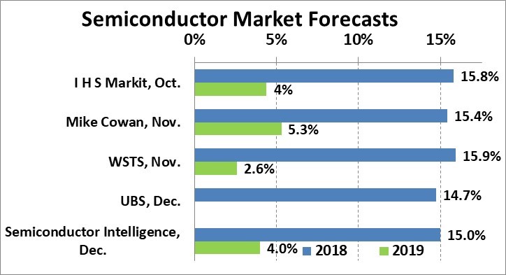
The chart below compares our latest forecasts with other recent forecasts. The consensus is the 2018 semiconductor market will finish with about 15% growth. All sources expect a significant growth slowdown in 2019. Most are in the 3% to 5% range in 2019. UBS projects a 4.3% decline in 2019 primarily due to a downturn in memory.

There are considerable downside risks to the forecast. Global GDP risks include the U.S.-China trade issues, Brexit, and rising interest rates. On the semiconductor side, the memory market downturn may be more severe than the flat market projected by WSTS. Previous booms in the memory market have usually been followed by double digit declines. However, since the significant memory suppliers have been winnowed down to three in DRAM and six in flash memory, the decline should not be as extreme as in previous cycles. The traditional major end equipment drivers of the semiconductor market such as PCs and mobile phones have shown little growth in the last few years. We at Semiconductor Intelligence will attend CES 2019 (previously known as the Consumer Electronics Show) in Las Vegas next month to look at emerging drivers of electronics and semiconductor growth.


Emulation Evaluation for the Ages!

Emulation Evaluation for the Ages!
by Daniel Nenni on 12-24-2018 at 7:00 am

One of the more entertaining things I get to observe in the semiconductor ecosystem is competitive customer evaluations of tools and IP. Seriously, this is where the rubber meets the road no matter what the press releases say.

This time it was emulators which is one of the most interesting EDA market segments since there is no dominant vendor. So it really is three big dogs eating out of one bowl as former Cadence CEO Joe Costello so elegantly put it many years ago. We all know Mentor dominates verification, Cadence AMS design, and Synopsys Synthesis and IP. But for emulation Mentor, Cadence, and Synopsys all have sizable dogs at this $300M+ bowl.

In my experience with emulation evaluations, if there is an incumbent (an already installed system) they have a distinct advantage, unless of course the customer has “outgrown” them which is what happened in this case. I had the inside track since I know Wave and have been waiting patiently for the press release to blog it:

Wave Computing selects the Mentor Veloce Strato platform for verification and validation of artificial intelligence SoC designs

“Wave Computing is revolutionizing artificial intelligence and deep learning with our dataflow technology-based solutions, which are pushing the boundaries of AI system design. The Veloce Strato roadmap not only addresses growing capacity needs, but it also maps to the diverse and expanding challenges of hardware/software verification and validation,” said Darren Jones, vice president of Engineering, Wave Computing. “When we saw that our reliance on hardware emulation was growing beyond early software validation, we evaluated all available tools. The Veloce Strato platform was the best solution that met our needs. It enables a robust virtual emulation environment that tackles complex AI design challenges.”

Coincidentally I was interviewed by CNBC last week and asked why smart phone companies are making their own SoCs instead of just buying them from Qualcomm. One of the reasons of course is emulation. When you design an SoC you can quickly debug the chip on an emulator then get started with software development before the silicon is back. Bigly advantage for a company like Apple who has lots of software floating around their SoCs, absolutely.

After talking to Jean-Marie Brunet, Director of Marketing, Emulation Division at Mentor Graphics, and getting some slides, I sent some questions to Darren Jones and Edmund Jordan at Wave:

Q: I would like to know why you chose Mentor?
We selected Mentor because the platform performed debugging processes far better, which is where we were spending the majority of our time. By helping us significantly reduce the amount of time we spent debugging, Mentor helped us speed time-to-market. Mentor’s Veloce® Strato™ emulation platform also included several different interface options and other features which led to Veloce being a far more complete solution, out-of-the-box.

Q: Can you elaborate on the details of your design?
We have a rather large design within a leading-edge process node. As is industry standard, we believe emulation is a key part of verifying design before the proposed solution is put on silicon, which is why we turned to Mentor’s Veloce® Strato™ emulation platform for assistance. Our design includes memory interfaces such as DDR, PCIE cards, etc. as well as a large array of custom processors.

Q: How fast did your design run on the emulator?
A rough estimate would be that we run about 1MHz, which is a notable improvement over what we ran on our previous product when debug is enabled. However, we use the emulator primarily for debugging the design so absolute speed is not as important as the speed of debugging.

Q: What is your chip design methodology?
We primarily use standard Verilog RTL, Synthesis, and place and route design methodologies. We do use custom blocks when performance is required.

Q: Is the chip taped out?
Yes.

Q: First silicon working?
Yes.

Q: Anything else interesting to add?
One advantage—and one of the reasons we chose Veloce—is that it’s very easy to use for hardware debug when running real-world software applications. What we liked most is that we could run different simulation cycles without having to recompile the design. This helps speed our development cycles, which is certainly advantageous.

We’ll always have simulation, but the advantage of emulation is it’s much faster than simulation. Thus, it enables us to run software that would take too long to run on a simulator. However, I’m certainly not going to run every software scenario on an emulator because doing so is not cost effective.

If you want to know who the incumbent was you will have to login and read the comments…


CAPEX Cuts and Microns Memory Markdown

CAPEX Cuts and Microns Memory Markdown
by Robert Maire on 12-21-2018 at 7:00 am

For those who have been paying any attention to the semiconductor industry its no surprise that memory demand and therefore pricing is down from its peak earlier in the year. Its not getting better any time fast.

After several strong years of demand and pricing, which was followed by enormous CAPEX spending we are seeing the standard reverse pattern of the cycle as we are headed back down to low pricing and low demand coupled with low capex. There still may be a few investors, inexperienced analysts and company management who still cling to “its no longer cyclical”, “its different this time” and “Santa Claus and the Easter Bunny are real…”.

Micron reported both EPS and revenue more or less in line with expectations with Revenues slightly low at $7.91B versus expected $8B and EPS slightly ahead of the expected $2.95 coming in at $2.97.

The big issue that caused the stock to drop after hours was guidance of $5.7B to $6.3B versus expectation of $7.3B. EPS is projected to be $1.75 +- $0.10 versus expected $2.44.

When memory slows down it goes off a cliff without skid marks……

We are somewhat surprised that other analysts did not cut their estimates in front of the quarter as it was obvious that things have been deteriorating for a long time. It was not rational to expect revenues to hold up given a double whammy of lower demand and lower pricing.

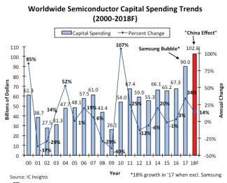
Capex was cut by about 12% at roughly $1.25B down. Bit growth in both NAND and DRAM sounds like the low teens in 2019. The company is cutting supply growth to match the reduced bit growth.

The one thing that is different this time is that Micron’s financial and cash position is much better and stronger to weather this downturn. The company spoke a lot about managing costs. Buybacks will help support the stock.

The company views this as an “air pocket” that will be short lived, perhaps the first half of 2019 given the underlying strong demand but we would be more cautious about all of 2019 rather than just the first half.

More impact on semi equipment companies
We think that the more negative impact that investors should focus on are the semi equipment companies. Though they may try to downplay the capex cuts as only $1.25B, the reality is that it is obviously much more widespread across the industry than just Micron.

Samsung capex memory spend down 75%??
We have mentioned previously that we have heard discussion of Samsung cutting its memory capex by as much as 75%. Given how much Samsung increased capex over the past couple of years, that level of cut would get them back to a more normal prior level. So the real concern is not Micron’s capex cut as Micron never went crazy but rather Samsung’s cut as Samsung was spending at way crazy, unsustainable levels.

Capex cuts will not be even- LRCX and AMAT suffer more
Micron made it clear on the call that they will keep up technology spending and slow capacity spending. The simple translation is spending on KLAC and ASML equipment and slowing dep and etch from Lam and Applied Materials. This does not mean EUV as memory uses standard DUV scanners but rather focus on going from 1X to 1Y then 1Z which requires yield management and lithography. Micron said its technology progress and costs were ahead of schedule.
Memory peaked at 84% of Lams business and we won’t see those levels again for quite a while

Micron, the stock, is still very cheap
The new estimate of $1.75 is an annual run rate of $7 which suggests the company is trading at roughly a bit over 4 times forward EPS, which is cheap by any standard.

The obvious question is what EPS will really trough at? If we trough at $1 a share per quarter , then we are currently trading at 8 times trough earnings. The next question is could we get below that? Whats the worst case scenario?
Given our guess that weakness lasts at least two quarters and perhaps more, we think $1 a quarter is likely a trough EPS.

Micron has a much better financial position in the current cycle than previous cycles with over $3B in net cash and an ongoing buy back program.

$30 feels like a pretty solid bottom in the near term for the shares of Micron. If the stock were below that we would be more aggressive buyers.

Much as we have seen recently, the after hours knee jerk reaction can sometimes reverse in the following trading day (as we had experienced with AMAT) so we don’t think the stock will be down as much as it was after hours.

Equipment stocks
Equipment stocks had a slight recovery only to retest lower levels. We think the Micron news is more negative for equipment companies than perhaps for Micron itself.

Lam remains the poster child or most direct victim of memory issues. We think the equipment companies could see more downside or limited upside as the real prospects of slashed Samsung spending come into view. Its quite clear that Samsungs spending in memory will be down, the only question is how much…..and we think that number is underestimated.

Quarterly outlook into 2019
Q1 is always the weakest quarter for the chip industry. With Chinese new year and a post partum depression after the holidays, memory pricing has historically been at its weakest.

Q2 may be a little better than Q1 but we see no reason for a bounce back.

Q3 2019 seems the earliest we could see any kind of recovery in demand and/or pricing of memory components.
The stocks may bounce along the bottom here for a while as we are in waiting mode.

With the addition of the China sword dangling above our head, upward movement in the near term is going to be very difficult at best.

This years new song….
Sung to the melody of “Baby Its Cold Outside”


Memory chips really can’t stay (Baby it’s cold outside)
NAND & DRAM prices have gone away (Baby it’s cold outside)
This long cycle has been (Been hoping that you’d dropped in)
So very nice (I’ll hold your hands they’re just like ice)
Investors will start to worry (Beautiful what’s your hurry?)
Stock prices haven’t found the floor (Listen to the fireplace roar)
So to cash I’d better scurry (Beautiful please don’t hurry)
Well maybe just a half a drink more (I’ll put some records on while I pour)

Synopsys Offers Smooth Sailing for OTP NVM

Synopsys Offers Smooth Sailing for OTP NVM
by Tom Simon on 12-20-2018 at 12:00 pm

Nobody likes drama. Wait, let me narrow that down a bit. Chip designers really hate drama. They live in a world of risk and uncertainty, a world that tool and IP vendors spend considerable resources trying to make safer and more rational. It’s notable just how ironic that Sidense and Kilopass were duking out patent litigation in the earlier part of the decade. Their products, one time programmable (OTP) non-volatile memory (NVM) exist solely to provide certainty and reliability in a wide range of IC’s – both digital and analog, from 180nm down to 16nm. It is noteworthy that both of these companies have been acquired by Synopsys – probably the EDA/IP company most renowned for its no non-sense approach to business and technology.

While usually a diversity of suppliers is a good thing for customers, these acquisitions have probably been for the better. Each of the two, Kilopass and Sidense, had their own strengths in this market, while both using similar 1T and 2T antifuse technology that has a lot to offer. Of course, there is more to OTP NVM than the bit cell, controller circuitry is also responsible for many aspects of the NVM memory block operation.

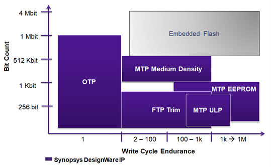
What are chip designers looking for when evaluating OTP NVM memory? In many cases OTP NVM is used for security related features, such as unique device identity, crypto key or secure boot code storage. It needs to be compact, cost effective, power efficient, secure and reliable. With the consolidation of this technology by Synopsys, customers should expect to have access to a full range of OTP NVM technologies. This ranges from small register size blocks up to megabit size storage for boot code.

Antifuse OTP NVM is easy to use because it requires no additional layers for CMOS processes. This helps manage production costs and risks. Antifuse also has some useful characteristics. Because the programming involves oxide breakdown during the write operation, it is nearly impossible to read the logic state through mechanical or visual inspection. Symmetric storage strategies also eliminate side channel attacks to read data. The oxide breakdown is also non-reversible, so it is not prone to EM driven metal regrowth, like eFuse can experience.

Also unlike the NVM techniques that use stored charge, antifuse NVM are not vulnerable to UV, thermal or aging issues that can lead to charge depletion and associated data loss. Antifuse is a robust and efficient method for OTP NVM. Larger instances can support few time programmable (FTP) which is implemented using remapping in the controller to provide re-write functionality. This is useful for trim information on PMIC, calibration on sensors, re-provisioning of security keys, or limited code updates, etc.

Synopsys, Sidense and Kilopass were all known for the extensive qualification work on a wide range of processes. A lot of sensor and analog chips use antifuse on older legacy process nodes, but Synopsys antifuse has been qualified on the latest FinFET nodes as well. This makes it attractive because other NVM techniques have had trouble migrating to smaller more advanced nodes.

Synopsys DesignWare OTP NVM is ideal for automotive applications because of its AEC-Q100 grade 0, 1, and 2 qualification. It has very high temperature stability, with operating temperatures up to 175C. Synopsys DesignWare OTP NVM is available on TSMC, SMIC, UMC, GLOBALFOUNDRIES.

Synopsys recently added an excellent overview of their full range of OTP NVM offerings and their advantages on their website. Despite the dramatic history, it seems that antifuse OTP NVM is a sound solution when looking for security, safety and optimal PPA.


AI at the Edge

AI at the Edge
by Tom Dillinger on 12-20-2018 at 7:00 am

Frequent Semiwiki readers are well aware of the industry momentum behind machine learning applications. New opportunities are emerging at a rapid pace. High-level programming language semantics and compilers to capture and simulate neural network models have been developed to enhance developer productivity (link). Researchers are pursuing various hardware implementations to accelerate throughput of both the dataset training and subsequent inference steps. These hardware projects include: a processor architecture for software-based execution of neural network models (CPU- and GPU-based); an ASIC specifically developed for ML applications (e.g., a TPU), or deploying commercial field-programmable logic arrays.

To date, however, the main production-level ML applications have been exercised on datacenter-class resources. The effective throughput is derived from evaluating the NN model on a batch of input samples, to compensate for the delays in loading the NN layer weights and activation functions from memory. Yet, the data is generated at the edge, and the connectivity bandwidth, latency, and power consumption to communicate with the central processing datacenter for inference evaluation simply does not scale. Thus, the R&D focus is shifting to innovations required in the (distributed) edge computing architecture.

The forecasts for the edge computing market are extremely robust – e.g., 35%+ CAGR, TAM exceeding $30B in 5 years. The application areas being pursued are diverse. (Although edge computing is often associated with the Internet of Things, I’ll stick with edge computing in this article – several of the application examples given below are not usually associated with the IoT.)

The most publicized edge computing AI activity is certainly the development work on autonomous vehicles. Another fast-growing ML area is in the field of factory automation and robotics. There are applications where a human operator is currently glued to a monitor, where machine learning technology can accelerate and alleviate the task of classification. Increasingly, video surveillance technology will incorporate more sophisticated ML inferencing computation. The detection of an attempted network intrusion security breach will also expand the adoption of ML decision support.[1]

An interesting area that I recently read about is the opportunity to provide emergency call centers and responders with more accurate information. Analysis and classification of various patient inputs (e.g., breathing, voice patterns) will improve the triage steps immediately pursued. In these examples, note that the primary characteristic is that the inferencing throughput must be optimized for batch = 1.

Perhaps the best indication of the tremendous growth and interest in edge computing for AI applications is the introduction of an industry conference specific to the topic – the Edge AI Summit – recently held in San Francisco. One of the presentations at the conference was from the team at Flex Logix, who provided details of their NMAX embedded FPGA IP, optimized for edge AI applications.

Last month, the Flex Logix team shared an overview of NMAX with me (link). Recently, I met with the team again to review the details of their Edge AI Summit presentation.

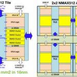
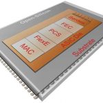
NMAX is a field-programmable logic architecture specifically developed for edge AI (batch = 1). The NMAX “tile” building block for embedded IP integration consists of:


  • MAC logic (64 8-bit MAC’s in each cluster, 8 clusters per tile)

From the detailed (floating point-based) training weights, the NMAX edge AI MAC utilizes a scaled int8 implementation, with minimal loss in classification accuracy.


  • traditional programmable logic

The activation function calculations for each neural network layer are mapped to this EFLX logic. The state machine control for layer-by-layer evaluation and NN model reconfiguration sequencing is also mapped to this logic.


  • internal L1 SRAM

The L1 SRAM stores the node weights – more on that shortly.


  • connectivity to embedded L2 SRAM

The composite NMAX tile array can be integrated with a range of L2 SRAM sizes (link). The L2 stores NN layer data values while the tiles are being reconfigured for successive layers. As will be discussed shortly, developers will optimize the tile array and SRAM configuration for their NN model.


  • high embedded IP I/O pin count for external connectivity

The goal of the NMAX implementation for edge AI is to minimize the number of (and latency to) external DRAM, to retrieve the layer configuration data, weights, and store intermediate results. Real-time NN object classification examples provided in the Edge AI Summit presentation illustrate images/second classification results on the YOLOv3 benchmark using only 2 LPDDR4 DRAM modules, achieving 24 fps with a 6×6 tile array plus 36MB L2 SRAM @ 1GHz. (YOLOv3 is a demanding image classification benchmark – i.e., utilizing >100 layers, >60M weights, requiring 800B calculations/image.)


  • compiler support, from a NN model description to full physical eFPGA programming

The figure below illustrates the functionality of the NMAX compiler. The user provides the NN model (e.g., TensorFlow, Caffe), and the proposed tile array plus SRAM topology.

The intermediate compiler output provides the allocation and sequencing of NN model layers to the hardware in the tiles, allowing the user to quickly optimize the area versus throughput tradeoff. The final compiler output data provide the physical programmable logic assignment and interconnect implementation throughout the tile array.

Specifically, the NMAX compiler addresses NN throughput using several unique algorithms. Cheng Wang, Senior VP of Engineering at Flex Logix, indicated that there are features to provide an optimal assignment of layer nodes to the tiles, as well as overlapping of model reconfiguration steps. For example, while a layer is executing, the weights for the next sequence of nodes to be configured are pulled from L2 SRAM (or external DRAM) into L1 memory. Once the next logic reconfiguration is complete, the corresponding set of node weights are transferred to L0 inside the tile MAC to execute.

Geoff Tate, Flex Logix CEO, indicated that his discussions with Edge AI Summit participants showed great interest in larger NMAX configurations, able to contain multiple NN layers in the tile array, executing in a direct pipeline without the latency of reconfiguring the tile logic and weights for successive layers.

FPGA logic offers a unique hardware alternative for ML applications, with improved performance over software-centric architectures. For the transition to ML inference at the edge, embedded FPGA IP is an excellent fit, as long as the following characteristics are available:

  • optimized for the high MAC demand
  • integrated with a significant capacity of L2 SRAM
  • wide connectivity to L2 and external DRAM to minimize latency to load new network input data and layer configuration information
  • expandable to allow optimization of area, power, and computational throughput (especially the ability to represent multiple network layers without logic reconfiguration)

The NMAX architecture from the Flex Logix team strives to meet these requirements for edge AI applications (link).

-chipguy

References

[1]Xin, Y., et al., “Machine Learning and Deep Learning Methods for Cybersecurity”, IEEE Access, Volume 6, p. 35365-35381, 2018.


DAC versus SEMICON ES Design West!

DAC versus SEMICON ES Design West!
by Daniel Nenni on 12-19-2018 at 12:00 pm

As I mentioned in a previous post, the big drama at last year’s Design Automation Conference was the acquisition of the Electronic Systems Design Alliance (formerly EDAC) by SEMI, the owner of the SEMICON West Conference franchise. The plan is to add an ES Design West wing to the SEMICON West conference in San Francisco next year. DAC is in June, SEMICON West is in July, thus the conflict. Given EDAC was a big DAC supporter some consider this a treasonous act which makes it all that more entertaining.

The timing is right to launch a competitive conference in San Francisco because in 2019 DAC will be in Las Vegas, a location criticized for a lack of local technical community support amongst other things. DAC has been in Las Vegas twice over the last 35 years if my memory serves me. The first time was in 1985. It was memorable as my second DAC but also because I was just married and my beautiful bride joined me. It really was an exciting time in EDA and Las Vegas is an exciting venue, absolutely.

In fact, my beautiful wife and I returned to Las Vegas 30 years later to renew our wedding vows. Funny story, we actually went to Las Vegas on our anniversary to see Elton John and I had planned on surprising her with a quick chapel reenactment by an Elvis impersonator but the hotel had a last minute wedding cancellation so we got a large room with all of the trimmings. My wife was duly impressed, Las Vegas baby!!!

Here is the official ESDA announcement:

Oct 24, 2018:ESD Alliance Announces ES Design West Debut in Conjunction with SEMICON West 2019 in San Francisco

One thing I can say about the Design Automation Conference organizers is that they listen and last week is proof in point. DAC will be in San Francisco from 2020-2025 and probably beyond. Talk about returning fire, wow! Truthfully, I will miss the exotic DAC venues like Las Vegas, New Orleans, San Diego, Los Angeles, Austin, Miami, Dallas, Albuquerque, and other locations that I attended but can’t recall.

But I do agree that the San Francisco DAC provides the most value add for EDA and IP vendors exhibiting their wares, absolutely. The question is: Will there be enough demand for two Design Automation Conferences in San Francisco a month apart in 2020 and beyond? You tell me in the comments section and I will add my thoughts.

Here is the complete DAC PR:

The Design Automation Conference Secures a Five-Year Conference Location at San Francisco’s Moscone Center

The world’s premier event devoted to the design and design automation of electronic chips to systems returns to the Bay Area starting June 2020 and beyond

LOUISVILLE, Colo. – December 13, 2018 Tapping into a resurgent interest in electronic design automation and the proximity to Silicon Valley, sponsors of the Design Automation Conference (DAC) announced they will hold the annual event, now in its 56[SUP]th[/SUP] year, in San Francisco for five consecutive years, starting in 2020.

DAC’s sponsors – the Association for Computing Machinery’s Special Interest Group on Design Automation (ACM SIGDA), and the Institute of Electrical and Electronics Engineer’s Council on Electronic Design Automation (IEEE CEDA) – secured the following dates at San Francisco’s Moscone Center to hold their annual event.

  • DAC 2020, June 17 – 26 – North and South Hall
  • DAC 2021, June 23 – July 2 – West Hall
  • DAC 2022, June 15 – 24 – North and South Hall
  • DAC 2023, June 21 – 30 – North and South Hall
  • DAC 2024, June 19 – 27 – West Hall

After 55 years, DAC continues to be the world’s premier event devoted to the design and design automation of electronic chips to systems, where attendees learn today and create tomorrow. A rise in attendance and participation in the 2018 DAC in San Francisco spurred the sponsors to return to the city after the 2019 event that will be held in Las Vegas, June 2-6. More than 6,000 people attended and more than 170 companies exhibited at DAC 2018 held at Moscone West Center.

DAC is the only event for top-notch researchers to present their cutting-edge discoveries, the platform for leading field engineers to share their experiences in using EDA (electronic design automation) tools to tame the ever-growing circuit and system design monsters, and the largest exhibition of EDA tools, software, IP cores, and other related products and services. DAC has been and will continue to be the must-attend event for the design and design automation community.

“We attend DAC to build our knowledge of what is possible so that we can continue to innovate and stay at the leading edge of design,” stated Chris Collins, senior vice president, products & technology enablement at NXP. “DAC has been and always will be a place we look to for such guidance. It is a place where we can meet with pioneers, innovators, and solutions providers to understand the technology and provide feedback on the technology that will drive our next products.”

The abstract submission deadline for DAC 2019 technical papers closed November 20, 2018, with a record 1049 abstracts received and 819 accepted papers for review. The number of accepted papers for review for DAC 2019 has surpassed the last five years of accepted for review papers by approximately 19%. Among the hot topics for 2019 are submissions in areas such as machine learning and artificial intelligence architectures, which increased by 61%.

“DAC continues to evolve to satisfy the needs of our industry. It’s always been the premier place for presenting EDA research and showcasing all vendors under one roof,” said John Busco, director, logic design implementation at NVIDIA. “In recent years, it’s added tracks to satisfy the interests of working designers and IP consumers. DAC brings together academia, commercial EDA, and electronic system designers—a true cross-section of semiconductor design. As technology progresses, and both our challenges and opportunities multiply, DAC offers an ideal forum to explore, exchange ideas, and innovate.”

The call for contributions for the 56[SUP]th[/SUP] DAC in Las Vegas is now open for the Designer Track and IP Track. The submission deadline is January 15, 2019. For more information visit: https://www.dac.com/submission-categories/designer-track

About DAC
The Design Automation Conference (DAC) is recognized as the premier event for the design of electronic circuits and systems, and for electronic design automation (EDA) and silicon solutions. A diverse worldwide community representing more than 1,000 organizations attends each year, represented by system designers and architects, logic and circuit designers, validation engineers, CAD managers, senior managers and executives to researchers and academicians from leading universities. Close to 60 technical sessions selected by a committee of electronic design experts offer information on recent developments and trends, management practices and new products, methodologies and technologies. A highlight of DAC is its exhibition and suite area with approximately 175 of the leading and emerging EDA, silicon, intellectual property (IP) and design services providers. The conference is sponsored by the Association for Computing Machinery’s Special Interest Group on Design Automation (ACM SIGDA), and the Institute of Electrical and Electronics Engineer’s Council on Electronic Design Automation (IEEE CEDA).

Design Automation Conference acknowledges trademarks or registered trademarks of other organizations for their respective products and services.


Ampere: More on Arm-Based Servers

Ampere: More on Arm-Based Servers
by Bernard Murphy on 12-19-2018 at 7:00 am

Since I talked recently about AWS adding access to Arm-based server instances in their cloud offering, I thought it would be interesting to look further into other Arm-based server solutions. I had a meeting with Ampere Computing at Arm TechCon. They offer server devices and are worth closer examination as a player in this game.


First, the people at Ampere are heavy hitters. Start with Chairman and CEO Renee James, a past president of Intel. The CFO/COO is ex Apple and Intel and almost everyone else is ex Intel, immediately or at some time in the past, including the architect and VP of engineering, all with solid server backgrounds. I’ve also heard that they are raiding Marvell/Cavium for talent. I met with Matt Taylor, SVP of WW Sales and Biz Dev. Between Intel and Ampere, Matt was VP of sales for Qualcomm’s Datacenter group. All in all, a pretty impressive lineup for a business targeting the cloud space. The company is funded by the Carlyle group (first round), though no word on how much.

I had to ask Matt for his view on why QCOM exited servers. No real surprises but good to hear from an insider. He said the business opportunity was strong (well he would), but QCOM was distracted (just a bit). Paul Jacobs and Derek Aberle, who were supporters, left and QCOM had to cut $1B, for which datacenter was an easy target. Multiple reasons, fairly unique to QCOM, which didn’t really say anything about the general Arm-based server opportunity.

Ampere is going after the same target as Annapurna (AWS), except Ampere isn’t captive so is aiming at all the cloud top-end providers (the hyperscalers/super 8) – Google, Amazon, Microsoft, Facebook, Baidu, Alibaba, Tencent, and China Mobile – all of who buy servers by the railcar load.

On specs, Matt has offered that in current 16nm implementations the Ampere eMAG solution is comparable to Xeon Gold devices, but at half the cost and Epyc devices at half the power. Side-note on power: some analysts think cloud users won’t care – they just pay for usage time, so performance should be the only metric that matters. Wrong – power contributes significantly to total datacenter overhead in the cost of keeping the whole thing cooled. Your bill as a user is part runtime (and price) on the instance type you chose and part overhead, including cooling costs. So yeah, power matters, even though it’s an indirect cost.

Lenovo has released (recently) their ThinkSystem HR350A rack server based on the eMAG processor, so it’s already possible to deploy servers based on the devices. Just like Arm, they stress scale-out applications (high parallel operations like video serving, where it is easy to add more processors to handle more parallel requests) and similar applications where performance per dollar and performance per watt are important considerations.

Matt told me that they are at various stages (eval to deployment) with big cloud service providers and are hearing similar themes for workload trends well-fitted to Arm-based servers, including storage, internal and external search, content delivery, in-memory db applications and (interestingly in china) for mobile gaming with cloud-based rendering. Some of these are accelerator options but he stressed also standard server applications with differentiated capabilities that you couldn’t easily get on the usual platforms. Sadly he didn’t want to share specific examples.

Overall, sounds very consistent with the Arm story I wrote about earlier. Arm-based servers may not be as fast, unit for unit, as the best of the best from Intel and AMD but (a) they’re a lot cheaper and lower power than those options and (b) you can build your own customized solutions optimized to higher throughput per dollar/watt for specific workloads. In some pretty high traffic datacenter applications, the best of the best may not always be the best total system solution.