Samsung is a complicated company with a VERY long history. We attempted to capture the Samsung Experience in chapter 8 of our book “Mobile Unleashed: The Origin and Evolution of ARM Processors In Our Devices”. If you are a registered SemiWiki member you can download a free PDF copy in our Books section.
Here is the chapter 8 introduction:
To Seoul, via Austin
Conglomerates are the antithesis of focus, and Samsung is the quintessential chaebol. From humble beginnings in 1938 as a food exporter, Samsung endured the turmoil and aftermath of two major wars while diversifying and expanding. Its early businesses included sugar refining, construction, textiles, insurance, retail, and other lines mostly under the Cheil and Samsung names.
Today, Samsung is a global leader in semiconductors, solid-state drives, mobile devices, computers, TVs, Blu-ray players, audio components, major home appliances, and more. Hardly an overnight success in technology, Samsung went years before discovering the virtues of quality, design, and innovation. The road from follower to leader was long and rocky.
And here are the final thoughts of the chapter:
A bigger question is how Samsung, and others, continue to innovate in smartphones beyond just more advanced SoCs. There are also other areas of growth, such as smartwatches and the IoT, where Samsung is determined to play. There are me-too features, such as Samsung Pay, and new ideas like wireless charging and curved displays. (More ahead in Chapter 10.)
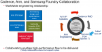
How this unfolds, with Samsung both supplier and competitor in an era of consolidation for the mobile and semiconductor industries, depends on adapting the strategy. Innovations in RF, battery, and display technology will be highly sought after. Software capability is already taking on much more importance. As Chinese firms improve their SoC capability, the foundry business may undergo dramatic changes – and the center of influence may shift again.
History says Samsung invests in semiconductor fab technology and capacity during down cycles preparing for the next upturn. Heavy investments in 3D V-NAND flash, the SoC foundry business, and advanced processes such as 10nm FinFET and beyond are likely to accelerate, and competition with TSMC and other foundries will intensify as fab expenses climb.
This book was published in December of 2015 and while there have been lots of changes at Samsung many things remain the same. Remember, they have the full support of South Korea including the government and more than 51 million people.
Bottom line: Samsung is a brute force technology innovator and we are very lucky to have them as a leader in the semiconductor industry, absolutely!
The Samsung Technology Day featured three key announcements introduced by the president of Samsung Semiconductor:
“Samsung is focused on harnessing the most advanced semiconductor technologies to power innovation across key markets,” said JS Choi, president, Samsung Semiconductor. “From System LSI devices that are perfectly adapted for real-world 5G and AI, to advanced solid-state drives (SSDs) that handle mission-critical tasks and offload CPU workload, we are determined to deliver infrastructure capabilities that are built to enable every wave of innovation.”
- Exynos 990 and 5G Exynos Modem 5123:Delivers unprecedented AI-powered user experiences on-device with a dual-core neural processing unit (NPU) and enhanced digital signal processor (DSP) that can perform over ten-trillion operations per second. The Exynos 990 and 5G Exynos Modem 5123 harness the most advanced chipmaking technologies to-date with a 7-nanometer (nm) process using extreme ultraviolet (EUV) lithography.
- Third-generation 10nm-class (1z-nm) DRAM:Delivers the industry’s highest performance, energy efficiency and capacity, since mass production in September. Optimized for premium server platform development, the 1z-nm DRAM will open the door to a lineup of memory solutions at the cutting-edge such as DDR5, LPDDR5, HBM2E and GDDR6 products as early as the beginning of next year.
- 12GB LPDDR4X uMCP (UFS-based multichip package): Combines four 24Gb LPDDR4X chips and an ultra-fast eUFS 3.0 NAND storage into a single package, breaking through the current 8GB package limit in mid-range smartphones and bringing more than 10GB of memory to the broader smartphone market.
Personally, I found the event well organized and the presentations very well done. They were personalized and entertaining. One of the comments was that Samsung will dramatically increase their cloud silicon business. Currently they have 0% market share so the sky is the limit, literally.