

A variety of growing and emerging segments of the semiconductor industry rely on Silicon-On-Insulator (SOI) wafers. Soitec is the primary source for SOI wafers particularly on 300mm. On Tuesday at SEMICON I got to sit down with Bernard Aspar, Soitec’s Executive Vice President, Communication & Power BU and Christophe Maleville, Soitec’s Executive Vice President, Digital Electronics BU and discuss what is going on at Soitec.
During SEMICON GLOBALFOUNDRIES announced they have reached $2 billion dollars of design wins on their 22FDX FDSOI platform that relies on wafers from Soitec and Soitec was clearly pleased by this development.
I started the interview by asking about Soitec’s financial health. A few years ago they were struggling. Soitec built significant 300mm capacity to support IBM’s partially depleted SOI (PDSOI) business. At one time all three major game console manufacturers relied on IBM PDSOI process for their main processor chips. Unfortunately, the value proposition of PDSOI wasn’t very good and all three console manufacturers moved away from PDSOI taking away the major driver of 300mm SOI. Last year at SEMICON West Soitec said they had returned to profitability and that has continued into this year. Over the last three years Soitec has refocused on their core business and they are now growing nicely (4% and 31% the last two years), in fact there are reports in the industry of SOI shortages.
I asked Soitec about their current capacity situation and they said the 200mm line is full and 300mm is significantly loaded. Siotec has 200mm and 300mm lines in France, a 300mm line in Singapore and a 200mm line at Simgu China. Capacity is currently tight but Soitec is investing in expanding capacity. They are contracting with their customers and contract customers aren’t suffering but if someone new wants large capacity it would take time. 300mm has grown 2x in the last two years. Soitec has >1.5 million wafers per year of 300mm shell capacity that is >50% equipped. Singapore will ramp up 300mm to follow market demand. 200mm is >1 million wafers per year.
RFSOI
IBM’s Burlington Fab is the leader in RF SOI for antenna tuning and switching in the front end of cell phones replacing more expensive GaAs solutions. With the acquisition of the IBM semiconductor operations by GLOBALFOUNDRIES more attention is being paid to this business. Each generation of cell phones, 2G, 3G and 4G required a new and more complex front-end while maintaining the front-end module from the previous generation for backwards compatibility. With 5G on the horizon even more complex 5G front-end modules will be added to phones along side 2G, 3G and 4G modules, see figure 1.
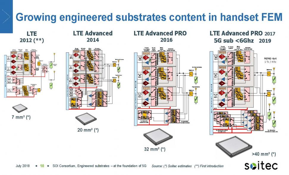
Figure 1. Mobile phone front ends.
GLOBALFOUNDRIES has recently repurposed their 300mm East Fishkill fab for RF and Silicon Photonics and is also introducing RF into their 300mm Singapore Fab. This provides Soitec with a nice long-term growth driver for RF SOI wafers in 200mm and 300mm.
FDSOI
The recent design wins announcement from GLOBALFOUNDRIES is another example of the growing acceptance of FDSOI. Where PDSOI married an expensive SOI substrate with a complex process and provided only moderate performance improvements, FDSOI offers a greatly simplified process to offset the expensive starting substrate. FDSOI also combines good logic density and performance with low power and excellent RF and analog performance. Both Samsung and GLOBALFOUNDRIES have FDSOI foundry processes currently available and next generation processes in the works (I will be writing more about this shortly). 5G and Internet Of Things (IOT) are two emerging applications where FDSOI is expected to be very successful. FDSOI is made on SOI wafers with very thin silicon layers of ~6nm on ~20nm buried oxide layers. Soitec has significant intellectual property in producing these demanding specifications with the required uniformity.
Silicon Photonics
Silicon Photonics has been in development for many years and is starting to gain traction. The need for very high speed/energy efficient data transport in datacenters is driving an effort to move optical interconnect down to the blade level creating significant unit volume. This is an emerging opportunity for Silicon Photonics (I will be writing more about Silicon Photonics in the near future). 5G is another emerging application for silicon photonics. Silicon Photonics processes are fabricated on SOI wafers with ~500nm silicon layers on 1 to 3 micron buried oxides.
Piezzo Layers
Soitec’s expertise in wafer bonding and thinning is also being applied to creating thin piezoelectric material layers on insulator (POI) for filter applications. The emerging 5G standard has tight signal specifications that need well controlled stable filters providing another application for Soitec’s core expertise.
Other Applications
Soitecs basic tool box of bonding and controlled layer thickness can also be applied to thicker SOI layers for power electronics. Bonding of novel III-V materials is another area where Soitec can apply their expertise to produce novel engineered substrates. For example, they can produce thin InGaAs layers on sapphire for micro display applications.
Figure 2 illustrates the different Soitec substrates to support the applications discussed above and figure 3 illustrates how the various substrate types support 5G.
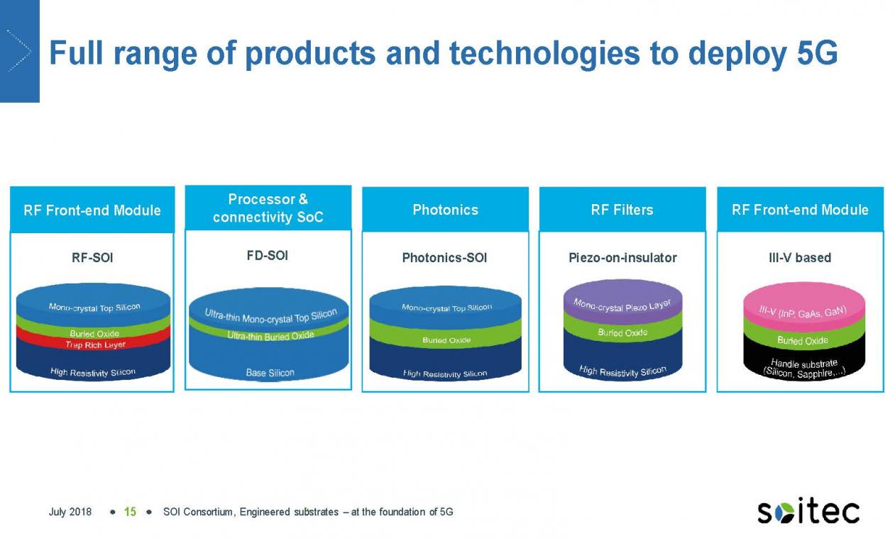
Figure 2 Soitec substrate options.
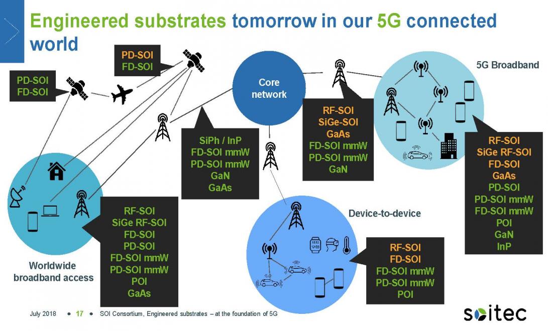
Figure 3. Soitec engineered substrates 5G usage.
Soitec – Leti Partnership
During SEMICON West Soitec and Leti announced the creation of a Substrate Innovation Center at Leti. Leti is a long-time pioneer in the development of SOI. The new center will bring together Soitec and Leti’s expertise with equipment vendors to drive further innovation with a prototyping line that can explore new processes that can’t be developed on active production lines.
Cost
Cost was at one time a big stumbling block for SOI adoption and I asked if SOI prices are still coming down. They replied that price has come down to no longer be a blocking point to go into foundry. New products come at a price in-line with value added. The standard 15 years ago was a GaAs front end for mobile phones, but then RF SOI provide a 2x cost reduction. FDSOI substrates are more expensive but provide simpler processes and solutions so they are cost competitive. SOI is not the severe price pressure/blocking point it once was.
Conclusion
Where Soitec was at one time reliant on PDSOI going into game machines, the company now has a portfolio of products addressing, automotive, wearables, mobile and cloud. With Soitec’s engineered substrates becoming a key enabler in these segments, Soitec is well positioned for sustainable growth.


The Silicon Shield Has Never Been Stronger!