

The electronics industry strives to continuously introduce new product innovation and differentiation. The ASIC market arose from the motivation to offer unique (cost-reduced) integration that was not realizable with commodity MSI/LSI parts. The SoC market evolved to provide even greater differentiation, integrating a diverse set of data/signal processing, storage, and high-speed interface communications functionality. SoC designs were supported by the availability of (soft and hard) IP from external suppliers, with the opportunity to define complex “systems-on-chip”.
Although the release of new processor cores and interface IP receive the bulk of attention, advances in the PPA characteristics of memory IP are just as vital to the ongoing progress in SoC architectures. Indeed, the percentage of die area allocated to memory arrays on current designs often far exceeds the area associated with new logic and IP re-use.
At the recent Design Automation Conference in Las Vegas, the theme of design differentiation was prevalent. The emergence of (and investment in) machine learning applications was represented by numerous presentations, ranging from high-performance accelerators for neural network training (with security features to detect adversarial/malicious inputs) to power-optimized “always on” inference engines at the edge. Time-critical applications were another emphasis at the conference, with presentations on unique architectures for the computational constraints of real-time systems with high-speed data streams.
With these emerging data-centric and power-sensitive applications, and thus a major requirement for optimized on-die storage, I was curious how SoC architects were seeking differentiation in the PPA metrics for their designs. At DAC, I had an opportunity to chat with Paul Wells, CEO, and Tony Stansfield, Principal Architect at SureCore, Ltd. about this question. Their insights were very enlightening, and somewhat unexpected. Paul indicated, “We are seeing a growing demand for custom SRAM IP.”
Traditionally, SureCore has provided SRAM compilation technology to customers. Their “PowerMiser” and ultra-low power “EverOn” compilers provided unique IP features:
- highly granular power states, with sleep mode capabilities segmented with the SRAM array banks and peripheral circuits, using a proprietary hierarchical global/local tiling strategy
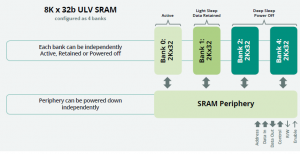
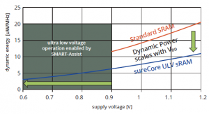
- ultra-low supply voltage operation for optimized leakage power, established at the array retention voltage (with voltage boost circuitry active during array operations)
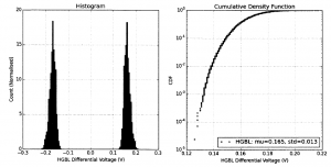
- comprehensive “high-sigma” sampled Monte Carlo verification methodology across PVT corners, especially important for ultra-low (retention plus boost) voltage operation
Paul said, “Given our expertise in SRAM IP compilation and power-optimized technology, customers are approaching us with requests for very unique implementations – for example, a 1W8R-poert array for a network fabric ASIC. We’ll use a 1W4R circuit design double-pumped during a read cycle.”
“For a very low standby power application, we’re able to employ our own array bit cell design, rather than the foundry bit cell. The array retention voltage is optimized, and verified to high-sigma. Although the bit cell is larger (using standard lithography design rules), the power and performance is optimized to the customer’s requirements – and, no array redundancy for DFY is needed.” Paul continued.
He summarized, “SureFit is the name for our custom SRAM IP design service. We are leveraging the compiler technology experience in SRAM design, characterization, verification, and industry-standard model generation, and applying that foundation to unique customer applications.”
Tony added, “Due to the modular and hierarchical architecture of the SRAM’s developed to support the internal power state granularity, there are unique opportunities to embed logic functionality with the array structure. With additional external signals, more complex functions could be readily integrated into the array, as well.” The potential performance and power improvements of in-memory computing was a hot topic at DAC. Although the majority of the conference presentations centered on adding logic to the base memory controller chip in an HBM stack with DRAM die, an SoC design seeking to aggressively minimize dynamic power would no doubt investigate “in-memory IP computing” opportunities, as well.
Is the era of “custom” hard IP design services upon us? Are the aggressive PPA constraints of emerging applications and/or the need for product differentiation driving a change in SoC design, with an investment in custom IP development? The SRAM IP team at SureCore certainly made a compelling case for this transition.
For more info about the SureFit services program, please follow this link.
-chipguy
Share this post via:


Comments
There are no comments yet.
You must register or log in to view/post comments.