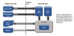
Artificial intelligence and machine learning (AI/ML) are working their way into a surprising number of areas. Probably the one you think of first is autonomous driving, but we are seeing a rapidly growing number of other applications as time goes on. Among these are networking, sensor fusion, manufacturing, data mining, numerical optimization, and many others. AI/ML is needed in the cloud, fog and edge. According to Silvaco in a recent webinar, the AI/ML market is going to expand dramatically over the next 5 or 10 years. This should come as no surprise, but the projections are impressive
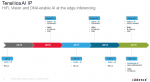
According to Silvaco there three mega trends driving the semiconductor market. The Smart Cities segment could be worth $1.4B by 2020. Smart City devices themselves will grow from $115M back in 2015 to $1.2B in 2025. The TAM for automotive semiconductors will reach $388B this year. The CAGR for the autonomous vehicle market is expected to be over 41% between now and 2023. For AI, with companies like Apple, Facebook, Google and Amazon designing their own AI chips, the market could easily reach $31B by 2025.
Since the term artificial intelligence was coined in 1956, up until a few years ago, it was characterized largely as an academic field of research. However, with the confluence of a number of key advances, AI/ML has taken off with astonishing speed. Silvaco’s Ahmad Mazumder, the presenter in the Silvaco webinar entitled “AI and Machine Learning SoCs – Memory and Interconnect IP Perspectives” talks about the main enablers for this rapid growth. He cites a number of silicon process technology developments such as strained silicon, high-K metal gate, FinFETs, and EUV lithography as contributing to this growth. The trend will be further accelerated by upcoming developments such as the GAA transistor.
Ahmad also brings up the issue of AI’s accelerated performance growth rate, in terms of GFLOPS, compared to CPUs and GPUs. Neural processing units (NPUs) offer scalability that goes beyond what other processors can achieve. As a result, there are an increasing number of AI/ML based SoCs that are going to be used in every type of computing environment. However, developing these SoCs requires addressing three major challenges: specialized processing, optimized memory and real-time interfaces for connections on and off chip.
AI/ML relies on efficient performance of several specific operations: matrix multiplication, dot products, tensor analysis, etc. Additionally, large bandwidth, high density and low latency memory is necessary for storing intermediate results as they move between processing layers. Finally, fast and reliable interfaces are required for transferring data throughout systems.
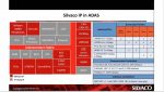
Ahmad points out that the growth in AI/ML related SoC development has caused a dramatic uptick in the demand for related IP, like that found in the Silvaco SIPware catalog. They offer IP in many of the essential categories needed for AI/ML based SoC development. The chart below shows Silvaco IP offerings for automated driving (ADAS).
The webinar includes an excellent overview of memory IP, including the JEDEC standards for DDR. We have seen widespread use of GDDR in AI/ML systems, but there are reasons to choose a variety of other types and configurations based on specific system requirements. Ahmad also dives into interface IP and how it plays a significant role in AI/ML systems, and he touches on Silvaco offerings for PCIe and SerDes. They offer IP for PCIe Gen4 and 56G PAM-4 PHY as part of their catalog.
The webinar drives home that point that AI/ML is becoming a major player in almost every kind of computational system, and in order to build hardware that fulfills its promise a wide range of IP needs to be readily available. The full webinar is available on the Silvaco website.