Last week, Cadence hosted its annual CadenceLIVE Americas conference. Four keynotes and eighty-three different talks on various topics were presented. The talks were delivered by Cadence, its customers and partners.
This blog is about the two keynotes delivered by CEO Lip-Bu Tan and President Dr. Anirudh Devgan. The guest keynotes from Partha Ranganathan, VP and Engineering Fellow from Google, and Dr. Yadunath Zambre, Chief Microelectronics Technology Officer (CMTO) of Air Force Research Laboratories (AFRL), are covered in two separate blogs.
While Lip-Bu’s talk provided the backdrop fueling the silicon renaissance, Anirudh’s presentation highlighted Cadence’s transformational product offerings the markets need now and into the future. If renaissance was the theme, allegro was the delivery pace of these keynotes. There were so many highlights that just one blog is not sufficient to cover everything that was presented. For example, the revolutionary Allegro X Design Platform deserves a standalone blog. This blog will include just a summary of that platform’s salient aspects.
Mr. Lip-Bu Tan’s Keynote
Lip-Bu opened his talk by calling out the five megatrends behind semiconductor growth. Then he proceeded to walk the audience through how these trends translate into secular growth drivers and ultimately how these secular growth drivers are behind Cadence’s product developments, investments, expansions, collaborations and partnerships.
The five megatrends are 5G communications, hyperscale computing, artificial intelligence/machine learning (AI/ML), autonomous vehicles and industrial IoT (IIoT). All these trends are connected by a common theme, which is data—data creation, processing, transmission, storage and analysis.
Data
Although most of the data nowadays is generated at the edge, only 20% is processed there. The rest of the data is transmitted to the cloud data center for processing, analysis and storage, and the results are sent back to the edge for taking action. This introduces several issues that can be grouped into three buckets: (1) Data privacy and security concerns, (2) cost and need for excessive network bandwidth and (3) intolerable roundtrip latency waiting for results for edge applications to act on. As a result, the edge is being treated more and more as a continuum with definitions of “near-edge” and “far-edge” capabilities that are needed, depending on the end applications. By 2030, 80% of data is expected to be processed at the edge. Depending on where in the edge spectrum processing happens, different types of solutions are required.
Drivers of Innovation
In addition to the above verticals/applications-driven semiconductor market forces, there are a number of secular growth drivers that are demanding innovations. For example, the slowing down of Moore’s law, lower yields from large dies in very advanced process nodes and reticle size limitations are leading to the disaggregation of SoCs. Heterogeneous chiplets integration, acceleration of 2.5D- and 3D-IC and chiplet-to-chiplet signal integrity analysis requirements are driving the need for transformational products from Cadence.
Cadence is leveraging its computational software expertise, massively parallel architecture and innovative algorithms to bring transformative products to its customers.
Dr. Anirudh Devgan’s Keynote
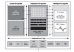
Anirudh opened his talk by defining three aspects that are critical to achieving what Cadence calls Intelligent System Design. He called them the three spheres that guide Cadence’s next wave of innovations and technology offerings. The spheres are pervasive intelligence (data), systems innovation (systems and software) and design excellence (chips, IP and EDA).
Staying true to its EDA, chip and IP roots, Cadence continues to maintain advanced-node digital implementation leadership. It boasts a count of 250+ 7nm/5nm tapeouts and industry’s first 3nm production plan of record (POR). It has also collaborated with Arm in implementing its first architecture for high-performance computing (HPC) servers. The Arm Neoverse-V1 processor can deliver mission-critical performance at 4GHz.
But today’s applications are demanding capabilities of the kind that in the past were used in aero/defense types of applications. Today, self-driving vehicles and advanced driver assistance systems (ADAS)-based vehicles need technologies similar to what an airplane uses. Many everyday applications are also moving toward leveraging multiphysics simulation and analysis.
Cadence has been investing heavily over the last few years in system-level innovations. It has expanded into the computational fluid dynamics (CFD) space through some key acquisitions—NUMECA and Pointwise. It is investing about 40% of its revenue into R&D. With about 5,000 people in R&D, a significant number of them are working on numerical analysis and computational software to connect the three spheres together. And the resulting solutions address the demands of a broad range of industries and market segments. Some of the market segments are consumer, hyperscale, mobile, communications, automotive, aero/defense, industrial and health.
Key Accomplishments Over Last Year
Design Excellence
The Palladium Z2 Enterprise Emulation and Protium X2 Enterprise Prototyping systems were launched. The Palladium Z2 emulation platform provides the best compile and debug times in the industry. The Protium X2 platform is FPGA-based to provide maximum flexibility to the customer in software bring-up and is the fastest system out there. AMD endorsed Cadence’s hardware platforms for helping with their top-of-the-line processor verification and software bring-up. NVIDIA talked about compiling and loading a multi-billion gate design emulation model in four hours compared to the 48 to 72 hours previous-generation platforms took.
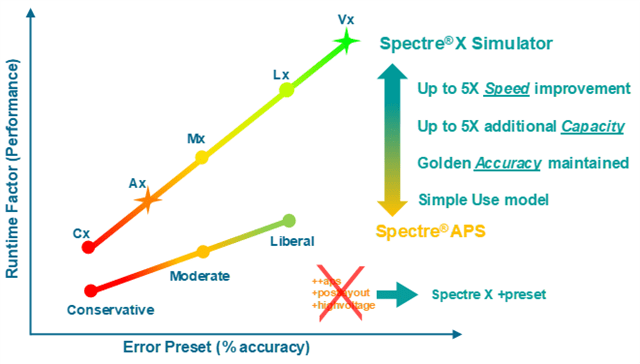
The Spectre FX Simulator, a next-gen FastSPICE simulator was released. This product is the result of a complete from-the-ground-up development to perform FastSPICE on memory structures. This capability was lacking in the venerable Spectre product that handles analog, mixed-signal and RF simulations. The Spectre FX Simulator is 3X faster than competing solutions and integrates with the Spectre platform to deliver a comprehensive solution to customers.
JVCKENWOOD endorsed Spectre FX capabilities in helping them get to market faster by about 40%.
Systems Innovation
AWR was acquired from National Instruments for its leading RF design platform for 5G and integrated with the Virtuoso and Allegro environments. Pointwise and NUMECA were acquired for their CFD system simulation capabilities. The Clarity 3D Solver Cloud was launched to cost-effectively and securely scale finite element method simulation capacity by providing easy access to compute resources in the cloud. The Celsius Thermal Solver integrates with the Clarity, Pointwise and NUMECA tools to provide the most accurate thermal analysis results. Recently, Cadence launched Sigrity X for next-generation power and signal integrity. Sigrity is the most widely used simulation tool for 2.5D, and Sigrity X delivers up to 10X performance on large-scale system analysis in the cloud. It can also be used with Clarity and Cadence PCB tools.
Allegro X Design Platform
Allegro, the packaging and PCB platform, is a very widely used platform that has been in existence for a long time with incremental enhancements along the way. The recently launched Allegro X platform is revolutionary and the biggest innovation in board and package design in almost two decades. It delivers much greater performance and data handling capabilities with the option to run on CPUs or GPUs.
If we were to highlight just three salient aspects of the Allegro X platform, they are:
- A unified cockpit for managing schematic capture, layout, SPICE simulation, signal and power integrity analysis, PLM integration, etc., compared to the previous-generation platform where users had to manually switch between different tools.
- ML-based P&R automation and integration with Sigrity technology and Clarity 3D Solver to deliver a 4X productivity boost and a 10X layout turnaround gain.
- A built-in data platform, called Allegro Pulse, for electronic system design data. Allegro Pulse can integrate with enterprise-level PLM systems for overall management.
Pervasive Intelligence and AI
Cadence believes its products deliver the best power, performance and area (PPA) benefits for its customers. Nonetheless, it continuously strives to improve. Through its AI/ML initiatives, it is working on ways to squeeze more efficiencies. It currently is in multiple beta engagements and is looking for additional beta partners.
Summary
Through its vision, focus and deep investments, Cadence has developed and is offering comprehensive and transformational products to its customer base. If you are involved in developing silicon, electronics hardware systems and software, you could benefit a lot by exploring and leveraging Cadence’s latest offerings.


