You are currently viewing SemiWiki as a guest which gives you limited access to the site. To view blog comments and experience other SemiWiki features you must be a registered member. Registration is fast, simple, and absolutely free so please, join our community today!
The new 5G C-band service is now up and running in the U.S., and subscribers are finally starting to see some of the promise of 5G. The new C-band services are primarily in spectrum allocations between 3 and 4 GHz, providing the wider channel allocation bandwidths necessary to deliver significantly higher data throughput. At the same time, signals at this frequency can travel significantly farther than with the mm-wave band. AT&T and Verizon customers are reporting download speeds ranging from 400 megabits per second (Mbps) to as much as 800 Mbps, a nearly 10x improvement over 4G LTE systems.
You can’t get this faster service at the airport though— at least not yet. The U.S. Federal Aviation Administration (FAA) has worked out a six-month agreement with the telecom providers to keep the C-band transmitters turned off near the affected airports due to ongoing concerns about the potential for interference with aircraft radar altimeters. During this time, the FAA continues to examine the radar altimeter systems used in commercial aircraft for certification, as well as to further study possible additional constraints needed for the nearby 5G C-band base stations.
Figure 1 – Verizon 4G/5G coverage map around the New York City airports, dated Feb. 24, 2022 (https://www.verizon.com/coverage-map/). The lighter colors around the airport indicate that lower-frequency 5G service is available within the region, but not the new Ultra Wideband (C-band) service.
This six-month hiatus currently affects about 500 towers nationwide at around 87 airports. As of Feb. 25, an estimated 90% of commercial airline aircraft have been approved for landing under the current agreement based on their radar altimeters’ ability to deal with interference from C-Band 5G base stations outside the airport zones on the 3.7-3.98 GHz bands. At some airports, the aircraft approved for landing takeoff and approach vary by runway, creating aircraft scheduling challenges between airlines and airport management. For example, at Chicago’s Midway International Airport, only one runway is cleared for 100% of the aircraft types served by the airport, whereas the other four runways are cleared for between 81% and 95% of aircraft types.
In July, Verizon and AT&T are expected to energize the C-band service towers for enhanced 5G service closer to, and perhaps including the airport campuses. During that time, the telecom service providers and the FAA will presumably have negotiated and settled on the acceptable parameters of operation for those new C-band 5G base stations. In addition, it is expected that the FAA will have completed testing on the radar altimeters that are currently in use throughout the aviation industry and their interactions with closer 5G towers.
How Simulation Can Help
It is somewhat surprising that this issue has come up when there are simulation tools such as Ansys EMIT which can predict these interference effects and provide guidance for mitigation. For difficult interference problems, the Ansys EMIT toolkit, an integral component of the Ansys Electronics Desktop and part of the Ansys HFSS portfolio, is designed to consider wideband transmitter emissions and assess their impact on wideband receiver characteristics.
Figure 2 – ” Ansys EMIT is an integral component of the Ansys Electronics Desktop and provides wideband interference simulation and mitigation for multiple RF systems and emission sources within a localized environment. EMIT is capable of utilizing high-fidelity installed antenna coupling data simulated by Ansys HFSS to capture wideband installed antenna-to-antenna couplings.”
When combined with accurate models for the radar altimeter antennas installed on host aircraft, and for the 5G base station antenna systems, we can form an accurate prediction of the maximum expected potential for interference. This interference prediction is useful for both in-channel conflicts as well as spectrum conflicts which might occur outside the radar altimeter band.
In this blog series, we will illustrate 5G C-band interference potential with a candidate radar altimeter system during an aircraft landing approach.
Examining the C-Band Spectrum neighborhood
Before considering simulation, let’s review first the spectrum situation in the C-band part of the radio spectrum.
Figure 3 – C-Band spectrum allocation showing the C-band 5G service channels (3.7-3.98 GHz) in proximity with the Aircraft Safety and Radar Systems band (4.0-4.4 GHz)
The 5G service providers purchased the rights to a country-wide spectrum from the FCC in December 2020 at a combined cost of $69 billion to gain access to up to 280 MHz of combined bandwidth. This allocation covers three separate 5G channels: – 3.7-3.8 GHz: Currently being phased in for current C-band tower deployments. This band is the primary subject of concern because it is being made available now. – 3.8-3.9 GHz: Future 100 MHz of spectrum that will be added to further increase capacity. – 3.9-3.98 GHz: Future 80 MHz of spectrum that will likely be added after the first two 100 MHz bands have been fully deployed.
So far, only the lowest channel with the greatest channel spacing from the altimeter band is being considered, but the closer (future) 5G channels may create even higher potential for interference between the two systems.
In our next blog installment, we’ll examine the 5G radio wideband emissions model and a candidate radar altimeter receiver model with wideband performance—essential ingredients to examining the in-band or out-of-band interference potential.
The growth of complexity for silicon test as it relates to test data volume and test times is driven by multiple concurrent factors. One dimension is simply the increase in silicon complexity. However, other factors are playing a role as well. These include higher reliability requirements for new applications such as automotive, aerospace and defense. These requirements have not only increased test challenges at the point of manufacture, but also are moving incipient test challenges to system assembly and assembled products in the field. Approaches that worked before are reaching their practical limits and new silicon lifecycle management test requirements are being tackled for the first time.
SiliconMAX High-Speed Access & Test IP + Synopsys TestMAX ALE Solution
To address these multiple issues Synopsys has developed an IP that allows the use of high-speed functional interfaces that already exist on chips for accessing the test network. This eliminates the need to set aside dedicated pins. This is especially true with high speed functional interfaces operating at speeds higher than test pins. Benefits of this approach are reduced pin count, less need for specialized test equipment, higher data rates and the ability to access test functionality at all phases of an SOC’s lifecycle.
Let’s dig into the details of this interesting shift in thinking. Many of us painfully remember when there were unique and specific interfaces for keyboards, hard drives, displays, pointers, printers, interface cards and the like. Once interfaces like USB and PCIe came along, it became obvious that consolidation made sense. Today’s SOCs all utilize interfaces such as USB and PCIe which can run at high speeds, so why not leverage as test access ports too? Furthermore, the IEEE 1149.10 specification approved in 2017 creates a standard for packetizing test data which can be moved through existing high-speed interfaces.
Synopsys is working on supporting 1149.10 protocol. TestMAX ALE test software from Synopsys pairs with SiliconMAX HSAT IP to provide a complete solution. Synopsys TestMAX ALE can run on testers, PCs or SLT platforms, doing ATPG pattern translation for data feeding into the SoC and reverse mapping for the data being collected from the SOC. SiliconMAX HSAT IP has the capability to support variety of interfaces like PCIe, USB, SPI, MIPI, 1149.10, etc.
SiliconMAX HSAT IP supports full test functionality. It handles data format translation, packetizing and depacketizing. It also conveys the test data and commands to the SOC’s DFT logic. Chips that use the SiliconMAX HSAT IP for test no longer need dedicated test pins. Time required to move data is reduced due to higher data rates of the functional interface. Plus, increased flexibility allows for improved reliability by supporting test throughout the entire lifecycle of the chip.
The SiliconMAX HSAT IP comes with the full set of collaterals needed to integrate it into a design. It uses a configurable ARM AMBA AXI slave interface to connect to the functional interface. Also included is ARM AMBA AXI loopback testbench generation. It also comes with configurable scan chains (512 max) and a TAP. There is an optional EBC interface for USB to enable DMA function. An added benefit is that SiliconMAX HSAT IP can also provide access to silicon monitoring network on SOCs.
Using existing high-speed interfaces for solves several important issues for SOC designers. It reduces or eliminates the need for dedicated pins and offers higher speed access to on chip scan and test resources. But perhaps most importantly it opens the door to improved silicon lifecycle management which is essential for many rapidly growing application areas, such as automotive. More information on SiliconMAX HSAT IP can be found here on the Synopsys website.
Moving deep learning from the cloud to the edge is the holy grail when it comes to deploying highly accurate, low-power applications. Market demand for edge AI continues to grow globally as new hardware and software solutions are now more readily available, enabling any sized company to easily implement deep learning solutions at the edge of the network, free from Internet connectivity, ensuring privacy, reliability, responsiveness and battery life.
Advanced audio interfaces, cutting-edge image recognition, and multi-axis motion and passive infrared sensing technology are enabling a new generation of security solutions for the smart home or enterprise. As a leader in deep learning technology, AI chip company Syntiant is hosting an upcoming webinar that will focus on building low-power, multimodal edge applications to ensure safety and privacy. Whether for smart home surveillance, medical devices, autos or industrial IoT, a panel of deep learning experts and engineers will demonstrate how image, sound and sensor applications can be run simultaneously at significantly low power.
Today’s machine learning approaches are enabling significantly higher accuracy for a litany of tasks where safety and privacy are paramount, like image and sound classification, object and person detection, condition-based monitoring, motion tracking and occupancy monitoring, natural language processing and medical data analytics. However, deployment of cloud-based deep neural networks often requires huge amounts of processing, memory and power consumption, which also are vulnerable to data breaches and higher latency. This webinar will focus on how to successfully deploy edge AI neural networks using Syntiant® ultra-low-power Neural Decision Processors™ that sense, analyze and autonomously act to allow mission-critical and time-sensitive decisions to be made faster, more reliably, and with nominal power consumption and greater privacy at the edge of the network. Learn how AI models for video doorbells, gunshot and glass break detection, occupancy monitoring, tamper detection, fire and smoke alerts, and so many more use cases can be easily deployed at less cost with designated latency, memory size and power consumption. The result is highly accurate, cloud-free inference, while minimizing false detections across myriad consumer and industrial IoT applications, from smart home security and medical devices to automobiles and aviation, among other use cases.
Learn More
The live webinar will be broadcast Wednesday, March 23 at 9 a.m. PST. Register hereto reserve a spot to learn more about edge AI deployment for safety and privacy applications, as well as find answers to probing questions, such as:
Are non-AI sensors creating a high rate of false detections?
Is excessive power consumption causing high budget costs?
Do space constraints limit design choices and implementations?
The market for edge AI is exploding and this exciting webinar will provide details for successful deployments. Research suggests that by 2028, 37 percent of the global infrastructure edge footprint will be for use cases associated with mobile and residential consumers, with the remaining 63 percent supporting applications in vertical markets such as healthcare, manufacturing, energy, logistics, smart cities, retail and transportation.
About Syntiant
Syntiant Corp. is a leader in delivering end-to-end deep learning solutions for always-on applications by combining purpose-built silicon with an edge-optimized data platform and training pipeline. The company’s advanced chip solutions merge deep learning with semiconductor design to produce ultra-low-power, high performance, deep neural network processors for edge AI applications across a wide range of consumer and industrial use cases, from earbuds to automobiles. Syntiant’s Neural Decision Processors™ typically offer more than 100x efficiency improvement, while providing a greater than 10x increase in throughput over current low-power MCU-based solutions, and subsequently, enabling larger networks at significantly lower power.
Read a SemiWiki CEO interview with Syntiant’s Kurt Busch here.
As a pilot and semiconductor professional I was a bit shocked to get an Airworthiness Directive due to the 5G rollout. Airworthiness Directives are legally enforceable regulations issued by the FAA to correct an unsafe condition in a product:
“Airworthiness Directive (AD) 2021-23-12 was issued for all fleets in December 2021 and was added to all fleet AOM/OM VOL I. Specific 5G airport/runway NOTAMs activated the operating provisions and restrictions contained in the AD. The FAA has issued 5G NOTAMs effective 12:00 AM EST on Wednesday, January 19, 2022. There are a significant number of 5G NOTAMs issued for airports throughout our system, to include our hub and gateway cities.”
We discussed the is detail in the SemiWiki Experts Forum: Airlines warn of ‘catastrophic’ crisis when new 5G service is deployed and I made some inquiries inside the semiconductor ecosystem of how this could possibly happen and how could it have been prevented. The best response I got was from Ansys who has been publishing blogs on the topic on SemiWiki and on their own website and there is more to come:
The latest post (above) included a video simulation (which is worth watching), the recent developments with the FAA, Verizon and AT&T, and how simulation could have avoided this Airworthiness Directive.
Caption – This computer simulation shows an aircraft landing through a C-Band 5G signal emitted from a base station near the airport. The orb below the aircraft represents the radar altimeter. Ansys, which created the simulation, is the leader in simulation software that is used by engineers to model these very types of scenarios so they can see and mitigate problems before physical products are made or deployed. This kind of modeling can also be used to set safety constraints on 5G transmitters at specific locations around airports or other locations of interest to public safety. It’s a lot less expensive to tweak a system in the computer than it is to make costly updates to hardware after construction. Shawn Carpenter, an expert in radio frequencies, antennas and 5G, is available to comment on the subject.
The FAA reached an agreement with Verizon and AT&T to delay activation of C-band service for six months on base stations near 50 commercial airports with low-visibility approaches. According to an FAA statement released January 28, the service providers shared information on the exact locations of new 5G transmitters so that the FAA can study interference potential in more detail to shrink areas where the wireless carriers are allowed to deploy active transmitters. At this point, it appears that C-band towers within 2 miles of the designated airports are still inactive, and it’s not yet clear when AT&T and Verizon will plan to activate them. Verizon has indicated that this affects about 500 towers near airports, which is less than 10% of their total deployment of new C-band systems.
The FAA has worked to approve radar altimeter systems as well as commercial aircraft on which they are installed, to allow low-visibility landings at airports where 5G C-band services have been deployed, subject to the agreement with the 5G service providers. By the end of January, the FAA estimated that it had approved about 90% of the U.S. commercial aircraft, including most large commercial jets that incorporate one of the 20 approved radar altimeter units. However, some smaller airports which can only be served by smaller aircraft are still experiencing flight cancellations because the aircraft servicing them have not yet been cleared.
As a pilot and frequent international flyer I still have concerns but I do appreciate the discussion and the efforts of ANSYS to better understand this problem, absolutely.
It’s one thing to lead an industry. It’s another to anticipate and meet a new challenge well ahead of competitors in an industry. It’s another thing, still, to solve a long-standing problem and receive barely a hint of credit.
Such is the case with General Motors’ semi-autonomous hands-free Super Cruise feature. While many of us are by now familiar with the hands free aspect of this novel solution, widely seen in Super Bowl commercials, fewer are aware of an entirely new capability that the system introduced to the market.
With the introduction of Super Cruise, GM has taken the lead in delivering what is described in the industry as a minimum risk maneuver (MRM) + stop in lane function. In other words, a driver using an active Super Cruise system will be saved from a crash by the system’s ability to detect inattentiveness and slow to a stop in its existing travel lane.
Interestingly, this Super Cruise side gig doesn’t appear to have a separate name and has yet to be called out or highlighted by GM. But a GM vehicle operating in Super Cruise mode will in fact slow down to a stop in its lane in the event of the driver’s incapacitation or willful inattention to the driving task.
The function is perfectly suited to the needs of drivers that may experience a medical emergency such as a seizure or heart attack. Car companies around the world have long sought solutions for detecting driver inattention or medical emergencies in the interest of automatically slowing and removing the car from the roadway – preventing any resulting death or injury from single- or multi-vehicle crashes.
This kind of safe, emergency functionality calls attention to two ongoing National Highway Traffic Safety Administration investigations of Tesla and Honda for unintended braking – attributable to either software glitches or sensor-related false positives. Teslas and Hondas are under investigation for stopping unexpectedly, sometimes at highway speeds, with a fully attentive driver at the wheel.
The irony of Tesla’s unintended braking – which has been widely noted for years prior to NHTSA stepping in – is the near impossibility of slowing or stopping a Tesla in the event of an unresponsive Tesla driver. On one or more occasions, police officers seeking to stop such a vehicle have had to position their cruisers in front of and around the offending Tesla in order to slow it to a stop by triggering its sensors.
GM’s attention to this particular application is reminiscent of the company’s Stolen Vehicle Slowdown function enabled by OnStar connectivity. OnStar, in collaboration with local law enforcement, can slow and stop a properly equipped stolen GM vehicle remotely as long as the vehicle is within eyesight of cooperating police officers.
The MRM + stop in lane functionality of Super Cruise is a harbinger of future semi-autonomous vehicle functionality tuned to the needs of an aging driving population. At least one company, Merlin Mobility, is seeking to bring such an aftermarket solution to the market while also extending its capabilities.
While the Super Cruise application is intended to slow and stop a vehicle in its existing travel lane, Merlin Mobility is seeking to deliver an aftermarket solution capable of pulling a car with an incapacitated driver out of the travel lane while also summoning emergency assistance.
Super Cruise, too, summons emergency assistance via its OnStar connection. According to Cadillac’s consumer-facing online messaging, the application works in the following manner:
FIRST ALERT
”If the system detects that you may not be paying attention to the road ahead, the steering-wheel light bar flashes green to prompt you to return your attention to the road.”
SECOND ALERT
“If the steering-wheel light bar flashes green for too long and the system determines continued lack of attention to the road ahead, the steering-wheel light bar flashes red to notify you to look at the road and steer the vehicle manually. Also, beeps will sound or the Safety Alert Seat will vibrate.”
THIRD ALERT
“If the steering-wheel light bar flashes red for too long, a voice prompt will be heard. You should take over steering immediately; otherwise, the vehicle will slow in your lane of travel and eventually brake to a stop, as well as prompt an Emergency-Certified OnStar Advisor to call into the vehicle to check on you. Super Cruise and Adaptive Cruise Control will disengage.”
The Merlin Mobility system operates in a similar fashion to GM’s Super Cruise except that Merlin Mobility claims that its system will call 911 operators (in the U.S.) directly and, as previously noted, will take over driving in the event of an emergency.
Merlin Mobility, which has yet to announce availability or pricing for its system, says it is based on a device installed on the inside of a vehicle’s windshield and is compatible with 100 vehicle models for aftermarket installation. Originally leveraging technology from Comma.ai, Merlin Mobility executives now hint that they have developed their own solution organically.
Both the GM and Merlin Mobility solutions point to potentially life-saving applications for semi-autonomous vehicle systems. Both demonstrate the creation of value from autonomous vehicle technology development that can be and is being realized in the market immediately. Now all GM has to do is give its application a name. Merlin Mobility’s system is called Copilot.
Dan is joined by Jonathan Friedmann, a serial entrepreneur and the CEO and co-founder of Speedata. Jonathan discusses the current challenges of big data analytics and how Speedata fits into the landscape.
The views, thoughts, and opinions expressed in these podcasts belong solely to the speaker, and not to the speaker’s employer, organization, committee or any other group or individual.
Frankwell Lin, Chairman of Andes Technology, started his career being as application engineer in United Microelectronics Corporation (UMC) while UMC was an IDM with its own chip products, he experienced engineering, product planning, sales, and marketing jobs with various product lines in UMC. In 1995, after four years working on CPU chip product line as business director, he was transferred to UMC-Europe branch office to be its GM when UMC reshaped to do wafer foundry service, he lead UMC-Europe to migrate itself from selling IDM products to selling wafer foundry service.
In 1998, after 14 years working in UMC, Frankwell switched jobs to work in Faraday Technology Corporation (Faraday), he lead ASIC business development then on-and-off leading ASIC implementation, chip backend service, IP business development, industry relationship development (IR), as well as Faraday’s spokesperson. In 2004 he started to lead the CPU project spin off operation of Faraday.
Frankwell became co-founder of Andes Technology Corporation in 2005 and he formally took the position to be Andes’ President since 2006 and got promoted as Chairman and CEO in 2021.
Frankwell received BSEE degree of Electrophysics from the National Chiao-Tung University, Taiwan, and MSEE degree of Electrical and Computer Engineering from Portland State University, Oregon, USA. Under his management, Andes has been recognized as one of leading suppliers of embedded CPU IP in semiconductor industry.
Andes also won the reputation of leading technology company with awards such like 2012 EE Times worldwide Silicon 60 Hot Startups to Watch, 2015 the Deloitte Technology Fast 500 Asia Pacific award, etc. Frankwell received accolade award of Outstanding Technology Management Performance, Taiwan, in 2015 and ERSO award in 2020 for his contribution to the high-tech industry. Frankwell is also the Board Director of RISC-V International since 2020.
What is the Andes Backstory?
Andes was founded in 2005. We have nearly 17 years of experience in the CPU IP business. We began by developing our own reduced instruction set architecture. As we watched the development of the RISC-V ISA, we found a great deal of similarity between our ISA and the RISC-V instruction set. As a result, Andes was able to seamlessly migrate our proprietary RISC to RISC-V gracefully without much pain.
What is the Andes history with RISC-V?
Andes began evaluating the open-source RISC-V ISA in 2014, a year before the founding of the RISC-V Foundation in 2015. We joined the foundation in 2016. Later, the foundation changed its name to RISC-V International Association.
Today, Andes is a board member. In RISC-V International, there are many task groups for various ISA development. We serve on several of them, including the SIMD DSP task group, which Andes chairs and we led the ISA development for the SIMD DSP extension, part of the standard RISC-V ISA.
The rapid market acceptance of our product line resulted from our ability to introduce RISC-V ISA CPU IP offerings ahead of competition. The design and verification procedures we built to ensure quality design with our original product line provided us an edge over competitors. They are using an open-source non-human readable hardware description language (HDL) to build their RTL. Andes designed RTL is human readable and developed using our well-established design and verification procedures. In addition, we have sales and support channels with 17 years of experience.
One example is the RISC-V Vector processor. We were the world’s first to make a commercial RISC-V Vector processor available in 2020. At that time, the vector ISA was still in the draft stage. When a ratified version 1.0 vector processor instruction set was announced, we updated our IP to meet the spec. The second example is the RISC-V DSP P extension. We developed IP based on a draft version of the Spec in earlier 2019 and will keep advancing the design when the P extension spec is ratified. Again, we were the first to deliver a commercial RISC-V DSP processor.
We’re experiencing rapid market adoption. Our default business model is IP licensing. Customers adopting our RISC-V IP to design their SOCs include the following. A couple of tier-one companies have designed Wi-Fi, Bluetooth, and IoT chips used in several different platforms. Picocom used our RISC-V core to design 5G base station. Similarly, EdgeQ has designed a 5G AI chip. Kneron has developed a machine learning AI Edge chip. HP Micro launched an MCU that can be used in AI Edge and other microcontroller applications. For the HPC (High Performance Computing) data center server market, we have several major wins at FAANG companies, but I cannot disclose their names. For security, one of our customers is a Silex Insight. For microcontrollers, Renesas was a major win for us.
The second business model is custom computing in which we enter into a signed agreement with customers to help them customize their special requirement based on one of our on-the-shelf RISC-V CPUs. Customers may require advanced features or instruction sets additions to make their CPU uniquely their own.
In 2021, Andes achieved a growth rate of 41 percent over 2020. For the first to third quarter of 2021, our preliminary EPS (earning per share) showed an increase of more than 300 percent. Our growth and profitability are built on two revenue engines. First our existing proprietary CPU business continues to produce license and royalty revenue. Second, our RISC-V product line is driving IP license and non-recurring engineering revenue and is quickly growing royalty income.
Can you explain how RISC-V is fundamentally different from Arm? What is the key characteristic?
The advantages that the RISC-V ISA brings are it is modularized, it is open sourced, and it started from a clean slate. Additionally, designers can add their own custom instructions. RISC-V begins with a base set of instructions then adds instruction modules: memory load store, integer, floating-point, vector processing, DSP etc. A minimum configuration for a very simple application may need only 200 instructions. From 200 to several thousand, different combinations of instructions provide RISC-V expansive flexible. Because the RISC-V ISA is open source, anyone can design their own CPU based on the RISC-V ISA, or they can license from commercial or even open-source resources.
Next, because RISC-V was designed from a clean slate, it has no burden at the beginning, the ISA has the architectural elements to serve the simplest IoT applications to the most complex AI-Deep Learning ones. Uniquely with the RISC-V ISA anyone can add their own custom instructions to accelerate computation of specific tasks in their design. Andes provides the EDA automation tools to designers add these custom extensions without impacting their design schedules
Where do you expect the most success in terms of design wins over the next couple to several years? Do you expect it to be broad based or do you expect more success in some applications over others?
Automotive is one application, others include AI, data center, 5G mobile application, etc. Also Flash memory storage such as SSD, end users SSD or enterprise SSD is another where we have had design wins. Recently, we have wins in high-speed, high-performance computing HPC. For example, optical computing integrated with traditional RISC computing. Another application is in display drivers, where the trend is to integrate the timing controller, the driver, and the touch panel controller into one chip.
RISC-V is also ideal in emerging markets as long as there’s no one dedicated market leader with dominant market share such as PCs and mobile phones. There will be three major industry standards in the next decade: X86, Arm, and RISC-V.
From a regional perspective, is it fair to assume that China is the fastest growing market for you when you think about the business for the next three to five years?
Okay, let me give you an example. Today, our revenue contribution from China was 25% in 2020. In 2021, it grew to more than 30%. In 2020, we did 26% in North America and 26% in 2021. The ratio from China is definitely growing. We’re expecting to see that its contribution in the 30% to 33% range.
China is drawn to RISC-V because it’s open source and they can control the architecture. The nature of the open source is no one alone will control your development. I think that’s important for their strategic thinking.
I’m looking at the list on the risc-v.org website, and I see Western Digital listed. Western Digital, is their SSD controller application the way they’re using RISC-V?
Yes, including but not limited. They also applied RISC-V to hard disk and other types of storage including but not limit to storage, they also open source their CPU to the world.
One other question, so are there any other companies that that have a very similar business model, as you guys in terms of offering RISC-V IP or are you pretty much the sole provider?
In RISC-V International there are 300 enterprise members and 2000 personal members. Let’s focusing on the 300 enterprise members. I believe about 10 of them are offering similar CPU IP products to the market. To name a few there is SiFive in the US, Codasip in Germany, Imagination Technology in the UK, CloudBEAR in Russia, Alibaba in China. In addition, there are several fully open-source suppliers such as UC Berkeley, ETH Zurich, and China Research Institute. Thus, customers can choose commercial CPU IP or open-source IP.
Does RISC-V hand have any IP that’s kind of aimed at replicating GPUs functionality or is it pretty much just focused on CPU architecture?
Imagination Technology is one of the candidates that that will incorporate RISC-V in GPU applications. But Imagination’s product is a RISC-V CPU coupling with their own display controller or GPU. However, RISC-V with vector extension is also available. You can leverage vector processing to do similar computation as found in the GPU application. Customers are leveraging our vector processor to combine with GPU to perform deep learning, display, and graphic computing.
How do the best RISC-V processors compare with Arm and X86 performance in terms of industry benchmarks?
To compare Arm’s product number with Andes product segments, the advanced processors we offer are in the same performance range from the low-end to the Cortex A53, A55. And we are developing out of order processors to achieve competitive advantage. Another vendor SiFive have processors in the same performance as the Cortex A72. They claim they will have a Cortex A76 level product offering later this year. I mentioned, Russian supplier CloudBEAR who claims to have an A76 class product available this year.
Manish Pandey, VP R&D and Fellow at Synopsys, gave the keynote this year. His thesis is that given the relentless growth of system complexity, now amplified by multi-chiplet systems, we must move the verification efficiency needle significantly. In this world we need more than incremental advances in performance. We need to become more aggressively intelligent through AI/ML in how we verify, in both tool and flow advances. To this end, he sets some impressive goals: speeding up verification by 100X, reducing total cost by 10X and improving the quality of result by 10 percentile points (e.g. 80% coverage would improve to 90% coverage). He sees AI/ML as key to getting to faster closure.
Background in AI/ML types
Manish does a nice job of providing a quick overview of the primary types of learning: supervised, unsupervised and reinforcement along with their relative merits. Synopsys verification tools and flows use all three techniques today. Supervised learning is the most familiar technique, commonly used for object recognition in images. This follows training on large banks of labeled images (this is a dog, this is a cat, etc). He points out that in verification, supervised learning is a little different. Datasets are much larger than bounded images and there are no standard reference sets of labeled data. Nevertheless, this technique has high value in some contexts.
In unsupervised learning there is no target attribute. Learning explores data looking for intrinsic structure, typically demonstrated in clustering. This method is well suited to many verification applications where no a priori structure is known. The third method is reinforcement learning, familiar in applications like Google’s AlphaGo. Here the technique learns it’s way to improvement across a succession of run datasets, such as it might see in repeated regressions.
Constrained random, CDC/RDC and formal
One important area where these methods can be applied is to identify coverage holes in constrained random (CR) analysis, then using AI/ML to find ways to break through. Difficult branch conditions can cause holes for example. Overcoming these barriers allows CR to expand coverage beyond that point. (I wrote about something similar recently.) Manish cited a real example where this technique was able to both substantially reduce time to target coverage by 1-2 orders of magnitude and to increase coverage over the pure CR target.
Another application is common in CDC analysis. Static analyses are infamous for generating say ~100k raw violations, generally rooted in a very small number of real errors. Unsupervised learning is an excellent approach to analyzing these cases, looking for clustering among violations. Between clustering and automated root cause analysis they were able to reduce one massive dataset to just ~100 clusters. This is easily a 100X reduction in time to complete analysis.
In formal analysis over a set of properties, orchestration is a way to manage distribution of proof tasks through selection of preferred proof engines over a finite set of servers. Reinforcement learning can greatly enhance this process through learning, to better order properties and engine assignments from one regression pass to the next. This they have seen deliver 10-100X speed up over default approaches to scheduling. Which in turn allows more time for verifiers to push for higher proof coverage.
Debug can benefit from AI/ML through automated root cause analysis a potentially huge benefit in compressing a very tedious task. Looking at past simulation results and debug action graphs through a combination of supervised and unsupervised learning, it is possible to identify top potential root causes by probability. Manish doesn’t quantify how much this reduces debug time, probably because that is highly dependent on many factors. But he does say the reduction is substantial, which seems entirely believable.
A holy grail in optimizing verification throughput is in finding a way to slim down testing in regression. Reducing to only those tests you need to run given any changes that have been made in the design. This is not an easy problem to solve, which makes it an obvious candidate for AI/ML. Manish talks about mining historic simulation data, bug databases and code feature data to determine test set reductions which should have minimal impact on coverage for a given situation. He doesn’t mention which methods he applied in this case, but I could see a combination of all three being valuable. He again suggests a large potential savings in time through this technique.
One last interesting example. Mapping from specification requirements to assertions is today a purely manual (and error-prone) task. Synopsys is now able to support this conversion automatically through natural language processing (NLP). Manish is careful to point out that success here depends on some level of user discipline in how they write their specifications. They support a workflow to help users learn how improve recognition rate. Once both users and the technology are trained 😃, conversion becomes an almost magical translation, again saving significant effort over the old manual approach.
This is real today
Manish closes by pointing out that they are already able to demonstrate the goals he set out at the beginning of his talk – substantial speedup in net runtimes with corresponding reduction in human and machine cost and improvement in quality of results over conventional CR coverage targets. He also stressed that these advances were hard won. They have been working on refining these capabilities, jointly with customers, over several years. AI/ML are not quick fixes, but they can deliver substantial gains in verification with enough investment.
In each move from 1G to 4G people became accustomed to seeing the new generation as primarily offering increased bandwidth and efficiency. It would be a mistake to view the transition to 5G along these same lines. 5G takes Radio Area Networks (RANs) from a use model primarily for cell phone communications to a service supporting multiple use models that can support industrial IoT, machine to machine, even real time applications such as automotive navigation and more. 5G comes with more new operational bands and modes that work in environments from rural to dense urban areas.
The 5G Evolution
The increased sophistication of 5G means major shifts in how mobile network operators (MNOs) build out and deploy their networks. An informative white paper by Achronix, a leading supplier of FPGA components and eFPGA IP, discusses the changes coming in 5G and how they will affect every aspect of its architecture. The paper is titled “Enabling the Next Generation of 5G Platforms”. Indeed, 5G is still in the processes of being specified. 3GPP, the organization that is developing the specifications, is currently on Rel-18, with plans for specification releases up to Rel-21 in 2028. Each release includes new features that add essential functionality.
Three New 5G Use Cases
5G adds three new use cases to the existing 4G fixed broadband implementation. The Achronix white paper describes them as follows:
Massive machine type communication (mMTC) supports machine to machine connections, with an eye towards large numbers of IoT devices requiring high efficiency, low cost, and deep indoor coverage.
Enhanced mobile broadband (eMBB) aims to meet the new requirements for interactive applications on mobile devices. The focus is on 8K streaming video, augmented reality and other high bandwidth uses.
Ultra-reliable low latency communication (URLLC) is the third use case focusing on high performance low latency real-time connectivity. It will be used for things like vehicle control, remote medical and time critical factory automation.
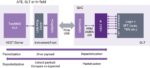
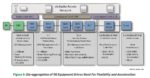
Because of the number of devices that will be connected and the new use models, the existing monolithic base station and backhaul building blocks will create bottle necks and limit flexibility. A new split architecture consisting of centralized units (CU), distributed units (DU) and radio units (RU) will be used. This change allows coordination for performance features, load management, and real-time performance optimization, which all enable adaptation to various use cases. DU, CU and RU elements can be collocated or physically distributed to accommodate the needs of the workloads and environment. This shift requires more intelligence in each type of equipment and the development of standard interfaces to allow a high level of interoperability.
5G RAN architecture
Where CPUs Fall Short, FPGAs Provide More Processing Power
It’s more than simply disaggregation that is driving the need to more intelligence and processing power within all elements of the 5G network. The white paper offers an excellent example of this on the expanding need for beam forming in the RU. Bandwidth is going from 20Mhz to 100MHz, transmission intervals are moving to 0.5ms and antenna arrays will grow to 64 by 64 elements. Future 5G releases will include AI/ML processing in the RU to improve signal quality. All of this will require significant processing power.
While it is tempting for the MNOs to fall back on virtualization of network functions running on traditional CPUs, the reality is that for systems far from the central office the requirements for power, cooling and size quickly begin to rule out multi-CPU solutions. With an evolving specification for 5G equipment, designing custom ASICs for DUs, CUs and RUs is not feasible. The Achronix white paper points out that FPGAs offer an excellent middle ground for these systems. They offer programmability and also provide high performance with very efficient power consumption.
FPGAs will allow upgrades on installed systems as new revisions are ratified. One additional way that Achronix offers to improve power and system size is by adding an embedded FPGA fabric to an ASIC. This eliminates costly and inefficient IO conversions between processing elements. Achronix eFPGA is fully configurable to specific system requirements, which means that no unused extra silicon real estate gets wasted. Furthermore, Achronix offers AI/ML processing units as part of their core functionality.
Every stage in the 5G radio area network (RAN) can benefit from the features offered by Achronix FPGA and eFPGA. The Achronix white paper dives deeper than I can in this article to illustrate the changes coming in 5G, both now and in future releases, and how Achronix FPGA and eFPGAs can effectively address them. The full white paper is available for download on the Achronix website.
From DIP to Advanced, semiconductor packaging has become strategic
For ease of reading – I am going to be splitting this primer into two parts. First is the technical overview of everything. Next will be the company-specific writeups that follow over time – specifically Teradyne, Formfactor, Advantest, and Camtek. Maybe Keysight and others over time. The concepts in this primer will likely be referenced over and over. This is a primer I wish someone had written sooner, as this will become a must-know in semiconductors going forward.
Why is Packaging Important Now
Packaging used to be an afterthought in the process of semiconductor manufacturing. You made the little piece of silicon magic, and then you attached it and moved on your merry way. But as Moore’s law has stretched, engineers realized that they could utilize all parts of their chip including the packaging to make the best possible product. Improving packaging gives you significant benefits, as there are thicker metal pieces for better conductivity, and I/O (input/output) problems are still one of the greatest issues for semiconductors.
What is more amazing is that none of the packaging companies were considered as important as the traditional front-end manufacturing processes in the past. The packaging supply chain was often considered “back-end” and viewed as a cost center, similar to the front office and back office in banking. But now as the front end struggles to scale geometry, a whole new field of focus has emerged, and this is the emphasis on packaging. We will discuss the variety of processes so you will never feel lost again while looking into this segment of semicap and understand what 2.5D or 3D packaging means.
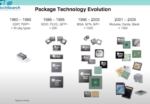
A Brief History of Packages
This is a brief hierarchy of package technologies I found from this wonderful Youtube lecture. If you have some time this series is worth a watch. Importantly it shows the hierarchy, of technology from past to present.
A simplified evolution is DIP> QFP > BGA > POP/SiP > WLP
There is clearly a lot of different package technologies, but we are going to go over the simplistic ones that broadly representative of each type and then bring it slowly to the present. I also really like this high-level overview below (it’s dated but still correct).
In the very beginning of packaging, things were often in ceramic or metal cans and hermetically (airtight) sealed for maximum possible reliability. This mostly applied to aerospace and military functions, where the highest level of reliability was required. However, this was not really feasible for most of our day to day use cases, and so we started to use plastic packaging and dual in-line packaging (DIP).
DIP Packaging (1964-1980s)
DIP was introduced in the 1970s and became law of the land for a decade before surface mount technologies were introduced. DIPs used plastic enclosures around the actual semiconductor and had two parallel rows of protruding electrical pins called leadframes that was connected to a PCB (printed circuit board) below.
The actual die is connected by bonding wire to two leadframes which can be attached to a printed circuit board (PCB)
DIP like so many early semiconductor inventions was created in 1964 by Fairchild semi. DIP packages are kind of iconic in a retro way, and the design choices are understandable. The actual die would be completely sealed in resin, so it leads to high reliability and low cost, and many of the first iconic semiconductors were packaged in this way. Notice that the die is connected to the external lead frame via wire, and this makes this a “wire-bonding” method of packaging. More on that later.
Below is the Intel 8008 – effectively one of the first modern microprocessors. Notice it’s iconic DIP packaging. So if you ever see those funky photos of semiconductors that look like little spiders, this is just a DIP package class semiconductor.
The original microprocessor from Intel, the 8008 family
Each of those little metal pieces then gets soldered onto a PCB where it makes contact with other electrical components and the rest of the system. Below is how the package is soldered onto a PCB board.
The PCB itself is often made of copper or other electrical components laminated by a non-conductive material. PCBs can then route electricity from place to place and let the components interconnect and talk to each other. Notice the fine lines between each of the circuits that are soldered to the PCB, those are embedded wires that serve as conduits from piece to piece. That is the “package” part of the packaging, and PCBs are the highest level of packaging.
While there are other renditions of DIP – it’s actually time to move onto the next paradigm of packaging technology that began in the 1980s, or Surface Mount Packages.
Surface Mount Packaging (1980s-1990s)
Instead of mounting the products via DIP, the next step-change was the introduction of surface mounted technology (SMT). As implied, the package is mounted directly onto the surface of the PCB and allows for more components and lower cost on a piece of substrate. Below is a picture of a typical surface-mounted package.
There are many variations of this package, and this was a workhorse for a long time in the heyday of semiconductor innovation. Something I want you to notice is that instead of the two lead frames that mount to the PCB, now there are 4 surfaces on all sides that are mounted. This follows the general desire of packaging, to take up less space and increase connection bandwidth or I/O. Each additional advancement will have that in mind and is a pattern to watch for.
This process was once manual but now is highly automated. Additionally, this actually created quite a slew of issues for PCBs such as popcorning. Popcorning the package is when moisture inside the plastic package is heated during the soldering process and the moisture causes issues in the PCB due to rapid reheating and cooling. Another thing to note is that with each increase in the packaging process there is an additional increase in complexity and failure.
Ball Grid Packaging and Chip Scale Packaging (1990s – 2000s)
As the demands of semiconductor speed continue to pick up, so does the need for better packaging. While QFN (quad-flat no-leads) and other Surface Mounted technologies clearly continue to proliferate, I want to introduce you to the beginning of a package design that we will have to know about in the future. This is the beginning of the solder balls – or broadly Ball Grid Array (BGA) packaging.
Those balls or bumps are called solder bumps/balls
This is what the ball grid array looks like and can directly mount a piece of silicon to a PCB or substrate from below rather than just taping down the corners on all 4 ends like the previous surface mounted technology.
So this is just another continuation of the trend I listed above, taking less space and having more connection. Now instead of a wire finely connecting the package on each side, we are now directly attaching one package to another. This leads to increased density, better I/O (a synonym for performance), and now the added complexity of how do you check to see if a BGA package is working. Up until this point, the packages were primarily visually inspected and tested. Now we can’t see the package so there was no way to test. Enter X-rays for inspection, and eventually more sophisticated techniques.
Solder bumps are also something I want you to remember as the primary way things are bonded to each other now, as this is the most common type of package interconnection pattern.
Modern Packaging (2000s-2010s)
We are now stepping into the modern era of packaging. Many of the packaging schemes described above are still in use today, however, there are increasingly more package types that you will start to see and those will become more relevant in the future. I will start to describe these now. To be fair many of these upcoming technologies were invented in previous decades, but because of cost, were not widely used until later.
Flip Chip
This is one of the most common packages you will likely read or hear about. I’m happy I can define it for you because I’ve never had a satisfying explanation in a primer I’ve read so far. Flip Chip was invented by IBM very early on and often will be abbreviated as C4. In the case of flip-chip, it really isn’t a stand-alone package form factor but rather a style of packaging. It’s pretty much just whenever there is a solder bump on a die. The chip is not wire bonded for interconnect but flipped to face the other chip with a connecting substrate in between, therefore “flip-chip”.
I don’t expect you to understand just from that awkward sentence, and I want to give you an example from Wikipedia, who has actually some of the best work on this I’ve seen. Let’s walk you through the steps.
ICs are created on the wafer
Pads are metalized on the surface of the chip
A solder dot is deposited on each of the pads
Chips are cut
Chips are flipped and positioned so that the solder balls are facing circuitry
Solder balls are then remelted
Mounted chip is underfilled with an electrically insulating adhesive
Wire Bond
Notice how flip-chip is different from wirebond. Remember that DIP package up top? That was wire bonding, where a die uses wires to be bonded to another metal that is then soldered to the PCB. Once again wire bonding is not a specific technology, but rather an older set of technologies that encompasses a lot of different types of packaging. I think it’s best described in relief to flip-chip. Wirebond is a precursor to flip-chip to be clear.
Honest if you’ve made it this far – you’re a champ. I think that really is all you need to know for this segment. There is a large number of variations of each form factor and just think of these as the overarching themes that dictate them. KLIC by the way is the market leader in this segment, and when you think of old packaging technology you should think of them.
Advanced Packaging (2010s to Today)
We are ever so slowly creeping into the “advanced packaging” semiconductor era, and I wanted to maybe touch on some higher-level concepts now. There are actually various levels of “package” that kind of fit within this thought process. Most of the packaging we have talked about before has been focused on chip package to PCB, but the beginning of advanced packaging really starts with the phone.
The mobile phone in a lot of ways is the huge precursor to so many aspects of advanced packaging. It makes sense! A phone in particular is a lot of silicon content in the smallest space possible, much denser than your laptop or computer. Everything must be passively cooled, and of course as thin as possible. Every year Apple and Samsung would announce a faster but more importantly thinner phone, and this pushed packaging to new limits. Many of the concepts that I will discuss began in the smartphone package and has now pushed itself to the rest of the semiconductor industry.
Chip Scale Packaging (CSP)
Chip scale packaging is actually a bit broader than it sounds and originally means chip-size packaging. The technical definition is a package that has no greater than 1.2x the size of the die itself, and it must be single-die and attachable. I actually have already introduced you to the concept of CSP, and that is through flip-chips. But CSP was really taken to the next level via smartphones.
The 2010s made CSP law of the land, everything in this photo is 1.2x the size of the chip die, and is focused on saving as much space as possible. There are a lot of different flavors of the CSP era with flip-chip, right substrate, and other technologies all part of this classification. But I don’t think knowing the specifics are of many benefits to you.
Wafer-level packaging (WLP)
But there is one level smaller – and this is the “ultimate” chip scale packaging size, or at wafer-level packaging. This is pretty much just putting the packaging on the actual silicon die itself. The package IS the silicon die. It’s thinner with the highest level of I/O, and obviously very hot and hard to manufacture. The advanced packaging revolution is currently at the CSP scale, but the future is all focused on the wafer.
It’s an interesting evolution, the package was something that got subsumed by the actual silicon itself. The chip is the package and vice versa. This is really expensive compared to just soldering some balls onto the chip, so why we are doing this? Why is there such an obsession with advanced packaging now?
Advanced Packaging: The Future
This is a culmination of the trends I have been writing about for a long time. Heterogeneous computing is not only the story of specialization, but how we put all those specialized pieces together. Advanced packaging is that crucial enabler that makes it all work.
Let’s look at the M1 – a classic heterogeneous compute configuration, specifically with their unified memory structure. The M1 to me is not a “wow cool” moment but a singular moment of pre and post for Heterogeneous compute. The M1 is ringing in what the future looks like, and many will be following Apple’s suit pretty shortly. Notice the actual SOC (system on chip) is not heterogeneous – but the custom package that brings the memory close to the SOC is.
This could be an edited photo – but notice the PCB has no wires – this is likely because of their awesome 2.5D Integration
Another great example of a very good advanced package is the new A100 by Nvidia. Once again notice no wires on the PCB.
Check this quote from their whitepaper.
Rather than requiring numerous discrete memory chips surrounding the GPU as in traditional GDDR5 GPU board designs, HBM2 includes one or more vertical stacks of multiple memory dies. The memory dies are linked using microscopic wires that are created with through-silicon vias and microbumps. One 8 Gb HBM2 die contains over 5,000 through-silicon via holes.A passive silicon interposer is then used to connect the memory stacks and the GPU die. The combination of HBM2 stack, GPU die, and Silicon interposer are packaged in a single 55mm x 55mm BGA package. See Figure 9 for an illustration of the GP100 and two HBM2 stacks, and Figure 10 for a photomicrograph of an actual P100 with GPU and memory.
The takeaway here is that the best silicon in the world is being made one type of way, and this revolution is not stopping. Let’s learn a little bit more about the words above and translate this into English. First some more about the two overarching categories of Advanced packaging, 2.5D, and 3D packages.
2.5D Packaging
2.5D is kind of like a turbo version of the flip-chip we mentioned above, but instead of stacking a single die onto a PCB, die are stacked on top of a single interposer. I think this graphic puts it well.
2.5D is like having a basement door into your neighbor’s house and physically is either a bump or a TSV (through silicon vias) into the silicon interposer beneath you, and that connects you to your neighbor. It isn’t faster than your actual on-chip communication, but since your net output is decided on the total package performance, the lowered distance and increased interconnection between the two silicon pieces outweigh the downsides of not having everything on a single SOC. The benefit of this is you can use “known good die” – or smaller pieces of silicon to piece together larger more complex packages very quickly. It would be better to all be done on one piece of silicon, but this process makes fabrication a lot easier especially at smaller sizes.
Those little pieces of silicon – are often called “chiplets” that you’ve heard all about. Now you can get chiplets of small functional blocks of silicon designed to be combined together, connect them on a single flat silicon substrate, and boom! 2.5D Package at your service.
Chiplets and 2.5D packaging are probably going to be used for a long while, it has a very workhorse like quality to it and likely will be easier to make than outright 3D and much cheaper as well. Additionally, it can scale well and can be reused with new chiplets thus making new chips in the same package format by just replacing the chiplet. The new Zen3 improvements are an of this, where the package is similar but some of the chiplets got upscaled. However this still kind of stops short at the final version of packaging, which is 3D
3D Packaging
3D packaging is the holy grail, the ultimate ending of packaging. Think of it this way, now instead of having all those separate little houses on the ground that are 1 story tall and connected by basements, we can just have one giant skyscraper that is custom made with whatever process is needed to fit the function. This is 3D Packaging – and now all the packaging is done on the piece of silicon itself. It is the single fastest and power-efficient way to drive larger more complex structures that are feature built to the task, and will “extend” Moore’s law significantly. We may not be able to get more feature shrink in the future, but now with 3D packaging we still could improve our chips into the future similar to Moore’s law of old.
And what’s interesting is we have a clear example of an entire semiconductor market that went 3D – Memory. Memory’s push into 3D structures is a very good indication of what’s to come. Part of the reason why NAND had to go 3D was that they struggled to scale at smaller geometry. Imagine memory as a large 3D skyscraper, and each of the floors is kept together by an elevator. These are called “TSV”s or Through silicon vias.
This is what the future looks like, and it’s even possible we will be stacking GPU/CPU chips on each other or stacking memory on CPU. This is the final frontier and one we are quickly approaching. You will likely start to see 3D packaging pop up over and over in the next 5 years.
A Quick Overview of 2.5D/3D Packaging Solutions
Instead of going much further into 3D and 2.5D packaging, I think it’s best to just lay out some processes that are being used and you might have heard before. I want to focus here on processes done by fabs, which are the ones that drive 3D/2.5D integration forward.
This is seemingly the workhorse of the 2.5D integration process and was pioneered by Xilinx.
This process is mostly focused on putting all the logic dies onto a silicon interposer, and then onto a package substrate. Everything is connected via microbumps or balls. This is a classical 2.5D structure.
This TSMC’s 3D Packaging platform, and is the relatively new kid on the block.
Notice this amazing graph on bump density and bonding pitch, SoIC is not even close to Flipchip or 2.5D in size and rather is pretty much a front end process in terms of density and feature size.
This is a good comparison of their technologies, but note that the SoIC actually has a chip on chip stacking akin to 3D stacking, instead of the interposer 2.5D integration.
Samsung XCube
Samsung has become a much more important foundry partner in recent years, and of course not to be outmatched Samsung has a new 3D packaging scheme. Check out the video for their XCube below.
There isn’t exactly a lot of information here, but I want to highlight that the A100 was fabbed on the Samsung process, so this is likely the technology powering Nvidia’s recent chip. Additionally of all the companies here, Samsung likely has the most experience with TSVs due to their 3D memory platform, so clearly, they know what they are doing.
Intel Foveros
Last but not least is Intel’s Foveros 3D packaging. We will likely see more implementations from Intel in their “hybrid CPU” process from their future 7nm and beyond generations. They have been pretty explicit at Architecture days that this is their focus going forward.
Something that is interesting is that there really isn’t much differentiation between Samsung, TSMC, or Intel in the 3D process.
Winners from the Advanced Packaging Revolution
So if you remember this post that was the introduction to the semicap series, Advanced packaging firmly is the “mid-end” that I reference. Why this is so interesting is because this is all incremental growth.
In the past, packaging estimates were excluded from WFE (Wafer Fab Equipment) estimates annually, but as of 2020, they are starting to include wafer-level packaging. This is kind of the signal for the wind shift and why the mid-end is very interesting from here. Another definition for Mid-end is Back End of Line (BOEL). For a more in-depth discussion of packaging-related companies, refer to my packaging stocks follow-up.
Subscribe to Fabricated Knowledge
Let’s learn more about the world’s most important manufactured product. Meaningful insight, timely analysis, and an occasional investment idea.


