The Federal Highway Administration in the U.S. tells us that “each year roughly one–quarter of all traffic fatalities and about one–half of all traffic injuries in the United States are attributed to intersections.” Intersections are clearly a challenge for human drivers, and the dirty little automotive industry secret is that intersections are an even bigger problem for computer-driven vehicles.
While humans run red lights – resulting in 700-800 fatalities annually – computer driven cars struggle to accurately identify the presence of traffic signals and stop signs and proceed appropriately without human assistance. Intersections are the great Achilles heel of autonomous driving – aside from all of the other weaknesses and unsolved problems these vehicles face – and remain an enormous challenge for transportation engineers.
One company, NoTraffic, has brought new thinking and new technology to municipalities. The two key insights that NoTraffic has employed are:
- Developing proper metrics for categorizing and quantifying the types of crashes that occur at intersections – left turn, rear-end, red-light running, right turn?
- Providing tools for communicating with drivers who are approaching intersections to alert them to the signal phase and timing of the light AND the potential for pedestrians in the crosswalk or a red light runner?
We hear a lot about connected cars these days. What we don’t hear much about is connected traffic lights and infrastructure. This is where NoTraffic comes in.
NoTraffic takes traditional disconnected infrastructure solutions – manifest in all those road-side boxes visible near traffic light installations – and digitizes them thereby allowing them to become part of a managed and always connected grid.
Nowhere is this transformation and its impact clearer than in NoTraffic’s approach to red-light runner mitigation. Rather than implementing enforcement cameras and the corresponding terror, confusion, and anger of impacted drivers, NoTraffic takes a more sophisticated, calibrated approach.
NoTraffic starts with measuring the extent of the problem. You can’t mitigate what you can’t measure.
NoTraffic breaks red-light runners into three “tiers:”
- Tier 1: A vehicle in the intersection during the yellow phase (light) with no conflicting green.
- Tier 2: A vehicle in the intersection during the red light, yet the intersection is in an all-red interval (no one has a green light).
- Tier 3 (most dangerous): A vehicle in the intersection during the red light and there is a conflicting green
Significantly, NoTraffic both measures and mitigates the problem – identifying troublesome times of the day when spikes in red-light running tend to occur – and then identifying solutions that typically do not require red light enforcement cameras.
Based on cameras plus Wi-Fi and cellular connectivity along with cloud-based analytics, NoTraffic’s solution provides three layers of safety benefits while also leveraging existing installations:
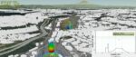
- A grid-level view into dangerous intersections, on a real-time basis, allowing cities to take precise measures – i.e. deploy local police to deter red-light runners at specific intersections and hours of the day (for example, intersections 1, 3, and 5, during rush hour traffic).
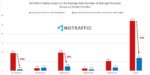
- Reduction in the potential for red-light-running crashes: by shortening delay times and queue lengths – in the example illustrated above, NoTraffic reduced the number of red-light runners, potentially minimizing the number of life-threatening crashes.
- Real-time notifications can be sent to road users by connecting urban intersections to a managed grid via their V2X-enabled IoT sensors, thereby enabling alerts to be sent to road users – connected vehicles, pedestrians, or cyclists – warning of vehicles about to cross an intersection on red, thus potentially minimizing the number of life-threatening crashes.
The data in the chart (above) represents a two-week window, gathered in April and May 2021 (two weeks in each month) in a major U.S. city where NoTraffic was deployed along a 1.8-mile corridor across five intersections. One of the intersections shows a slight increase during the mitigation period, which might be “noise” or lower cycle length for the reversible lane.
Most important of all, NoTraffic’s connected infrastructure solution is capable of communicating via cellular wireless technology with approaching vehicles or nearby pedestrians to warn of an identified red-light runner.
This is the future of connected infrastructure – with intersections connected to one another and to approaching vehicles and pedestrians. NoTraffic is more than a little ahead of its time – or maybe it’s right on time. The NoTraffic solution offers the promise of reducing the number of red-light runners or at least warning drivers and pedestrians when they occur. Perhaps just as important, the NoTraffic approach will lend a helping hand to hopeless autonomous vehicles.
Also read: