
At the recent VLSI Symposium on Technology and Circuits, Dr. Y.J. Mii, Senior Vice President of Research and Development at TSMC, gave a plenary talk entitled, “Semiconductor Innovations, from Device to System”. The presentation offered insights into TSMC’s future R&D initiatives, beyond the current roadmap. The associated challenges of the technologies being investigated were also highlighted. This article summarizes Dr. Mii’s compelling presentation.
Technology Drivers
Dr. Mii began with a forecast for future end market growth, emphasizing both the need for continued gains in high-performance compute throughput and the focus on power efficiency. For the HPC requirements, he shared a “digital data boom” forecast, shown in the figure below. For example, a “smart” factory will be expected to collect, monitor, and analyze 1 petabyte of data per day.
The role of machine learning (training and inference) support for the applications above is likewise anticipated to expand as well, putting further demands on the HPC throughput requirements. Dr. Mii commented that these HPC requirements will continue to drive R&D efforts to increase logic density, both in the semiconductor process roadmap and advanced (heterogeneous) packaging technology.
The relentless focus on power efficiency is exemplified by the slide below.
The architecture shown illustrates not only the extent to which 5G (and soon, 6G) will be pervasive in the devices we use, but also in the operation of “edge data centers”. As with HPC applications, the influence of machine learning algorithms will be pervasive, and needs to be focused on power efficiency.
Recent Technology Innovations
Before describing some of TSMC’s R&D projects, Dr. Mii provided a brief summary of recent semiconductor process technology innovations.
- EUV lithography introduction at node N7+
- SiGe pFET channel for improved carrier mobility
- Design Technology Co-optimization (DTCO)
Dr. Mii emphasized how process technology development has evolved to incorporate much greater emphasis on DTCO, that evaluating tradeoffs between process complexity and design improvements has become an integral part of process development. He highlighted recent adoption of contact-over-active-gate and single diffusion break process steps as examples. He added, “DTCO efforts are not exclusive to logic design – memories and analog circuitry are a key facet to DTCO assessments, as well.”
- nanosheets (at node N2)
TSMC will be transitioning from FinFET devices to a nanosheet device topology at the N2 process node.
Future Semiconductor Technology Innovations
Dr. Mii then described several semiconductor technology R&D efforts for future application requirements.
- CFET (complementary FET)
After decades of planar FET device technologies, FinFETs have experienced a considerable longevity as well, from N16/N12 to N7/N6 to N5/N4 to N3/N3E. It will be interesting to see how process nodes based on nanosheet devices evolve. After nanosheets, Dr. Mii focused on the introduction of CFET devices.
As illustrated in the figure below, a CFET process retains the benefits of the gate-all-around nanosheets, yet fabricates the pFET and nFET devices vertically. (In the figure, the pFET is on the bottom, and the nFET is on the top.)
In the cross-section of the inverter logic gate depicted above, the common gate input and common drain nodes of the two devices are highlighted.
The figure below expands upon the process development challenges introduced by the CFET device stacking, especially the need for high aspect ratio etching and related metal trench fill for the vertical connectivity highlighted above.
NB: Different researchers investigating CFET process development have been pursuing two paths: a “sequential” process where pFET and nFET devices are realized using a upper thinned substrate for top device fabrication that is bonded to the starting substrate after bottom device fabrication, with an intervening dielectric layer; a “monolithic” process where there is a single set of epitaxial layers used for all devices on the substrate. There are tradeoffs in process complexity and thermal budgets, device performance optimizations (with multiple substrate materials in the sequential flow), and cost between the two approaches. Although Dr. Mii did not state specifically, the comments about high AR etching and metal fill would suggest that TSMC R&D is focused on the monolithic CFET process technology.
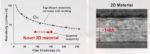
- 2D Transistor Materials
There is active research evaluating “post-silicon” materials for the field-effect transistor channel. As shown below, as the device gate length and body thickness of the channel are reduced, 2D materials offer the potential for both improved carrier mobility and sub-threshold slope (with lower leakage currents and the potential for lower VDD operation).
One of the major challenges to 2D process development is to provide low contact resistance connections to the device source/drain nodes. Dr. Mii shared results previously published by TSMC researchers highlighting the evaluation of bismuth (Bi) and antimony (Sb) – a 5X reduction in Rc over previously published work was achieved, as shown below.
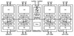
- BEOL interconnect architecture
Scaling of the back-end-of-line interconnect is encountering the challenge that existing (damascene) Cu wires are less effective. The Cu diffusion barrier (e.g., TaN) and adhesion liner (e.g., Ta) in the damascene trench occupies an increasing percentage of the scaled wire cross-section. The Cu deposition grain size is constrained as well, resulting in greater electron scattering and higher resistivity. The figure below highlights TSMC R&D efforts to introduce a new (subtractive-etched) BEOL metallurgy.
With a subtractive metal process, new opportunities for fabrication of the dielectric between wires are introduced – the figure above illustrates an “air gap” cross-section within the adjacent dielectric.
- 2D conductors
Beyond a replacement for Cu as the BEOL interconnect described above, TSMC R&D is investigating the potential for 2D conductors.
The figure above shows a cross-section of 2D conductor layers, and the resulting conductivity benefits compared to a comparable Cu wire thickness.
(Dr. Mii did not elaborate on the specific materials being evaluated. For example, there are a number of transition metal compounds that demonstrate high carrier mobility in a 2D crystalline topology, as well as the capability to stack these layers which are bound by van der Waals forces.)
Summary
Dr. Mii concluded his talk with the slide shown above. Future system designs will leverage:
- increased transistor density, as exemplified by CFET devices (and DTCO-focused process development)
- new interconnect materials
- increasing integration of heterogeneous functionality in advanced packaging, including both chiplets and HBM stacks in 2.5D and 3D configurations
- new methodologies for system design partitioning, physical implementation, and electrical/thermal analysis
It couldn’t be a more exciting time to be in the industry, whether as a designer or a process technology engineer.
-chipguy
Also read:
TSMC 2022 Technology Symposium Review – Advanced Packaging Development
TSMC 2022 Technology Symposium Review – Process Technology Development
