RVN! 26 Banner revised (800 x 100 px) (600 x 100 px)

Data Processing Unit (DPU) uses Verification IP (VIP) for PCI Express

Data Processing Unit (DPU) uses Verification IP (VIP) for PCI Express
by Daniel Payne on 03-29-2022 at 10:00 am

Fungible min

Domain specific processors are a mega-trend in the semiconductor industry, so we see new three letter acronyms like DPU, for Data Processing Unit. System level performance can actually be improved by moving some of the tasks away from the CPU. Companies like Xilinx (Alveo), Amazon (Nitro) and NVIDIA (BlueField) have been talking about DPU architecture for awhile now, and the SmartNIC is now being called a DPU in the hyper-scale data centers.

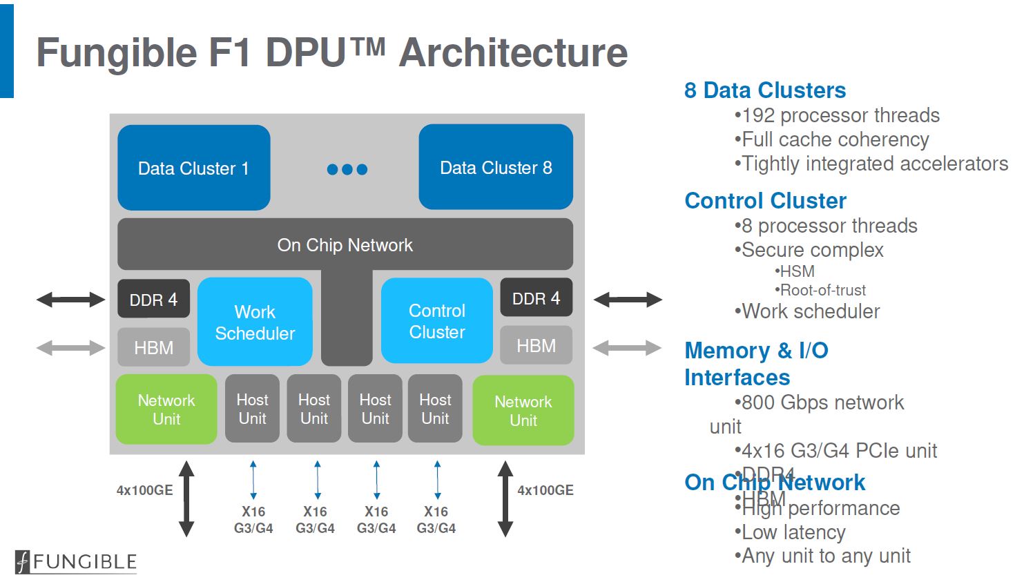
Last month I read about a new company, Fungible, as they announced their own DPU, and for verification of the PCI Express they used VIP from Avery Design Systems. Fungible presented their F1 DPU architecture at the Hot Chips conference, and here’s the block diagram where PCIe is on one side, and Ethernet on the other:

Source: Hot Chips


To learn more about DPU and PCI Express VIP I scheduled a Zoom call with Chakravarthy Kosaraju, SVP, Silicon Design and Validation at Fungible, and Christopher Browy, VP of Sales/Marketing at Avery Design Systems. In the big picture of things the CPU used to be powerful enough to handle all networking tasks, but now with so much data traffic it simply overwhelms the CPU cycles, so both the SmartNIC and DPU approaches are growing in popularity to get around CPU bottlenecks.

Disaggregation is the big trend in the data center now, because it allows more efficient use of resources like storage and data. CPUs paired with GPUs are trying to coordinate all the other PUs. The PCIe slot handles data between the server and storage. The Fungible F1 DPU goes into a storage server, manages all of the SSDs, and even handles cryptography.

Avery Design Systems and Fungible have been working together for the past 3-4 year on PCIe VIP.  On the VIP side the engineering team at Avery have now developed support for over 60 protocols, where PCIe is just one of their high speed IO protocols. The PCIe standard started way back in 2003, created by Intel, Dell, HP and IBM; now the specifications are managed by the PCI-SIG, a group of 900 companies.

When using PCIe in a SoC, you really don’t want to re-invent the wheel by hand-coding your own VIP, because it takes too many man-years of effort to do so, and Avery has been involved with the PCIe standard since version 1.0, and now we’re up to version 6.0 of the spec. Avery is a member of the PCI-SIG, and has many customers using their PCIe VIP, so that provided the team at Fungible the confidence to choose Avery for the version 5.0 VIP.

The team of globally dispersed verification engineers at Fungible were able to readily contact Avery with support questions about their new VIP.  Fungible used VIP from Avery,  among others, for its F1 DPU project. Complimentary feedback was provided by Fungible regarding the helpfulness of the VIP output files for debugging, the usefulness of the tracker files, appreciation for the extensive protocol checks, the speed of switch enumeration they experienced, and the ability to verify a system topology with ease. The F1 chips came back working successfully on first silicon; proving VIP improved their success rate. There are over 100 customers using the PCIe VIP from Avery, which speaks volumes about its stability and value.

The VIP from Avery is sold as time-based licensing, and has a flexible spending model (monthly remixing). Every simulation checks out both a simulator and VIP license for users.

The latest PCIe version is 6.0 right now, and there have been two updates already, even before full approval by the PCI-SIG. Typically Avery will do a quarterly update for VIP, tracking the standards so that all features are implemented. They have thousands of test cases and protocol checks, plus bug fixes and patches are part of their normal procedure.

Summary

Fungible was able to get first silicon success using a methodology of IP and VIP re-use on their F1 DPU chip, aimed at the datacenter market. Choosing Avery Design Systems as a partner for PCIe VIP was part of a multi-year relationship between the companies, and I expect them to continue that into the future.

Related Blogs


Path Based UPF Strategies Explained

Path Based UPF Strategies Explained
by Tom Simon on 03-29-2022 at 6:00 am

Path Based UPF Semantics

The development of the Unified Power Format (UPF) was spurred on by the need for explicit ways to enable specification and verification of power management aspects of SoC designs. The origins of UPF date back to its first release in 2007. Prior to that several vendors had their own methods of specifying power management aspects of a design. The IEEE 1801 specification that emerged has become widely accepted by designers and EDA tools that are related to power. Each new revision of the IEEE 1801 specification has worked to clarify and improve the effectiveness of UPF.

Yet, with such a novel and comprehensive scope, ideas that initially seemed workable have shown to have weaknesses. The very fact that there is no guarantee of backwards compatibility between revisions of IEEE 1801 shows that the working committee is willing and able to update and improve aspects of the specification that experience has shown need to be changed. One such area that was highlighted during a presentation at the 2022 DVCon by Progyna Khondkar from Siemens EDA. His paper and presentation titled “Path Based UPF Strategies Optimally Manage Power on Your Designs” clearly and concisely covers the changes in 3.0/3.1 relating to strategies for UPF protection elements such as isolation, level shifters and repeaters.

Previously the UPF syntax and semantics used to specify the location of isolations, level-shifters or repeaters, which are used between power domains to ensure proper operation of the circuit, were ad hoc and port based. In specifying the location of these protection elements or cells, there are a few kinds of potential problems that can arise – failure to insert a needed element, incorrect insertion of an element or duplicate placement of an element. The expansion in semantics from port based to path based is a significant change that addresses all of these issues.

Path Based UPF Semantics

UPF has added explicit use of -sink and -diff_supply_only TRUE to control inferring UPF protection cells. This is coupled with new precedence rules to eliminate unnecessary cells. Previously port based semantics allowed port splitting, which led to redundant UPF protection cell insertion. Now port-splitting is an error. UPF protection elements can be placed along a net so that only connections to specified sinks are made.  This leads to the placement of UPF protection elements as close to the sink domain as possible.

There are a lot of nuances to this change in UPF. The Siemens paper and presentation do an excellent job of going through various scenarios to illustrate the effects of using various path based options, while also comparing them to how port based semantics would perform.

There are three context options that can be used for UPF protection elements: -location self, -location parent and -location fanout. They have a profound effect on protection element placement. At the same time, they allow very precise tuning of this placement and remove ambiguity – leading to more precise results. The Siemens paper goes through each of them with illustrative examples to show how they differ. There is also a comparison of how the effects of the location directives are influenced by the choice of port or path based semantics.

There is a lot to absorb with this change. Tools supporting path based UPF protection elements need to perform consistently and also issue meaningful warnings when there are going to be unexpected results. The author suggests an approach for this. The paper and presentation conclude with a number of caveats and suggestions for designers switching to path based semantics. However overall it looks as though this is a welcome addition that will improve design quality and verification efficiency. The paper and presentation are available at the DVCon 2022 website.

Also read:

Co-Developing IP and SoC Bring Up Firmware with PSS

Balancing Test Requirements with SOC Security

Siemens EDA on the Best Verification Strategy


CEVA PentaG2 5G NR IP Platform

CEVA PentaG2 5G NR IP Platform
by Kalar Rajendiran on 03-28-2022 at 10:00 am

Pentag2 Programmable Accelerators Page 1

There are currently a number of attractive markets for technology oriented businesses to pursue. One such area is the 5G cellular market with opportunities to develop products for many use cases. A recent Ericsson Mobility Report forecasts incredible growth opportunities for various use cases within the cellular market. For example, cellular IoT connections are expected to grow from 1.9 billion in 2021 to 5.5 billion in 2027. Fixed Wireless Access (FWA) connections are projected to grow from 90 million in 2021 to 230 million in 2027. With such high-growth market opportunities, many semiconductor companies and systems OEMs are already pursuing various use cases for offering products. Many companies are also pursuing new entrance into this market. With 5G New Radio (NR) as the radio access technology for 5G mobile network, market success relies on rapid, cost-effective implementation.

All businesses desire a few things that are essential for profitable growth, no matter what markets they compete in. Those few things are: Easy development efforts at low costs. Rapid time to market for their products. Not wanting to be captive to high cost suppliers. And, of course easy entry for themselves into attractive market segments. The 5G cellular market is no different and a Software Defined Radio (SDR) based implementation may appear to be a good approach to play in that market. But the downside of SW centric implementation is power consumption. A key aspect of 5G NR specification is its focus on significant enhancements to solution flexibility, scalability, efficiency and power usage. A hardware implementation approach can deliver well on these aspects and does not have to be cumbersome and cost-prohibitive.

The above is the context for a recent product announcement from CEVA. Their PentaG2 5G NR IP platform substantially lowers barriers for semiconductor companies and OEMs to enter the cellular market segments. As the leading licensor of wireless connectivity, smart sensing technologies and integrated IP solutions, CEVA was the first to offer a 5G NR IP platform (PentaG) back in 2018. The platform has found wide adoption and has shipped in millions of 5G NR smartphones and mobile broadband devices to date. The current announcement is the 2nd generation of the platform and includes all the key building blocks for a full LTE/5G modem design.

The following provides some insights into the PentaG2 5G NR IP platform.

Optimizing Modem Processing Chains

The PentaG2 IP platform integrates low power DSPs with many specialized programmable accelerators for optimal modem processing chains. The accelerators are used for a complete end-to-end acceleration of uplink and downlink processing for both data and control channels, offloading the DSP cores from all data-path operations. Platform is still highly flexible by using efficient DSP controller cores to configure the HW elements. Each accelerator comes with standard AXI interface for ease of integration and allowing customers to add their own IP and secret sauce. Accelerators can be directly cascaded to form modulation and demodulation chain pipelines, without any need to buffer or access the DSP core for each operation.  The platform includes a complete L1 SW functional implementation of the main 5G Rx and 5G Tx processing chains. The result is a 4X improvement in power efficiency over its predecessor, the PentaG platform. Refer to the Figures below for the various CEVA accelerators included with the PentaG2 platform.

DSP Capabilities

The platform also includes field-proven low-power scalar and vector DSPs. The scalar DSP is used for PHY control, hardware acceleration scheduling and running the protocol stack. The vector DSP with 5G ISA extensions is used for channel estimation related workloads.

Current PentaG2 Platform Configurations

The PentaG2 platform is currently offered in two configurations. Both configurations allow for customers to incorporate their proprietary algorithms and IP as the platform supports standard AXI interfaces.

The PentaG2-Max configuration is for supporting eMBB use cases in handsets and CPE/FWA Terminals and mmWave, NR-Sidelink and cellular V2X (C-V2X) applications as well as URLLC enabled AR/VR use cases.

The PentaG2-Lite configuration is a compact and lean implementation, supporting reduced capability (RedCap) use cases including LTE Cat1 and future 3GPP Rel 17/Rel 18 RedCap. This platform configuration is ideally suited for tight integration into SoCs and for the IoT.

To learn more details, visit the PentaG2 product page.

Support for Simulation and Emulation

The PentaG2 platform deliverables include System-C simulation environment for modeling and debugging the designs. The PentaG2 SoC simulator interfaces with MATLAB platform for algorithmic development. A PentaG2-based system can be emulated on a FPGA platform for final verification.

Availability

PentaG2 is immediately available for licensing to lead customers and for general licensing in the second half of 2022.

Intrinsix IP Integration and Design Services

Customers can implement their PentaG2-based SoC using their in-house chip design teams or leverage CEVA’s Intrinsix IP integration services division. CEVA acquired Intrinsix in 2021 to bring additional offerings and services to its customer base. An example of a recent such offering is the CEVA Fortrix™ SecureD2D IP for securing communications between heterogeneous chiplets. Read more about SecureD2D IP here.

Also read:

CEVA Fortrix™ SecureD2D IP: Securing Communications between Heterogeneous Chiplets

AI at the Edge No Longer Means Dumbed-Down AI

RedCap Will Accelerate 5G for IoT


Analog Bits and SEMIFIVE is a Really Big Deal

Analog Bits and SEMIFIVE is a Really Big Deal
by Daniel Nenni on 03-28-2022 at 6:00 am

SemiFive Analog Bits SemiWiki

Given the recent acquisitions the ASIC business is coming full circle as a critical part of the fabless semiconductor ecosystem. The most recent one being the SEMIFIVE acquisition of IP industry stalworth Analog Bits. These two companies came to the industry from opposite directions which make them a perfect match, absolutely.

Analog Bits was founded in 1995 here in Silicon Valley the traditional way. Started by a group of engineers as a consulting company. In 2003 they pivoted to an IP company in concert with the foundries. This was a bootstrap operation (no debt) focused on customer success. I don’t recall my first engagement with Analog Bits but it was many years ago and for the last 4 years we have collaborated on SemiWiki.

Analog Bits is a critical supplier of leading edge mixed signal IP in the SoC, mobile, hyperscale, AI, and automotive communities. They started with PLLs, DLL, IO’s and memory IP, and have expanded to include SERDES, PVT, and POR. They are now serving customers down to 3nm which means intimate foundry relationships.

They have customers all over the world but more importantly Anaolg Bits is closely partnered with the top foundries: TSMC, Samsung, Globalfoundries, UMC, and had a recent announcement with Intel Foundry Services. As a foundry person myself I know the inside story here and let me tell you that it is an amazing achievement for a 50 person company.

SEMIFIVE took the opposite approach. After getting his PhD in Computer Architecture from MIT in 2012, Brandon Cho spent five years at Boston Consulting Group in Korea. In 2018 he joined SiFive in Korea and SEMIFIVE was spun out eight months later. Brandon and company have raised more than $100M in Korea thus far and now with a Silicon Valley based IP division (Analog Bits) expect them to raise more funds in California.

Here is a 2020 video explaining more about SEMIFIVE and what they do:

After the Analog Bits acquisition, SEMIFIVE has more than 350 employees and a solid base in North America. My prediction is SEMIFIVE will raise more money outside of Korea, do more acquisitions, and evolve into a multinational ASIC powerhouse.

They key to the ASIC business of course is IP and foundry relationships. SEMIFIVE has a close relationship with Samsung but does not currently work with TSMC. Analog Bits works closely with all foundries but has a very close relationship with TSMC. Seriously, it seemed like every time I was in Taiwan the Analog Bits team was there. To ensure these relationships continue unaffected by the acquisition Analog Bits will operate separately to remain foundry neutral.

Bottom line: To me this acquisition is another 1+1=3. SEMIFIVE gets a strong IP base in North America plus foundry and customer relationships that have been silicon proven for 20+ years. Analog Bits gets the ability to scale rapidly and increase the depth and breadth of their IP offering.

About SEMIFIVE
SEMIFIVE is the pioneer of platform based SoC design, working with customers to implement innovative ideas into custom silicon in the most efficient way. Our SoC platforms offer a powerful springboard for new chip designs and leverage configurable domain-specific architectures and pre-validated key IP pools. We offer comprehensive spec-to-system capabilities with end-to-end solutions so that custom SoCs can be realized faster, with reduced cost and risks for key applications such as data center or AIenabled IoT. With a strong partnership with Samsung Foundry as a leading SAFETM DSP partner, as well as the larger ecosystem, SEMIFIVE provides a one-stop shop solution for any SoC design needs. For more information, please visit www.semifive.com.

About Analog Bits
Analog Bits, Inc. is the leader in developing and delivering low-power integrated clocking, sensors and interconnect IP that are pervasive in virtually all of today’s semiconductors. Products include a wide portfolio of precision clocking macros PLLs and XTAL and RC Oscillators, Sensors to monitor Temperature, Voltage Drops, Voltage Spikes, System Power Integrity with integrated or separately available bandgaps and ADC’s. We connect the logic voltage of synthesized digital logic to external physical world using our unique programmable interconnect solutions, such as multi-protocol SERDES, C2C I/Os and differential transmitters and receivers. For more information, please visit analogbits.com.

Also Read:

Low Power High Performance PCIe SerDes IP for Samsung Silicon

On-Chip Sensors Discussed at TSMC OIP

Package Pin-less PLLs Benefit Overall Chip PPA


Auto Safety – A Dickensian Tale

Auto Safety – A Dickensian Tale
by Roger C. Lanctot on 03-27-2022 at 10:00 am

Auto Safety – A Dickensian Tale

As I prepare to join the International Telecommunications Union’s Future Networked Car Symposium – today through Friday – I am reminded of Charles Dickens’ “A Tale of Two Cities” and its unforgettable opening paragraph – modified for a modern context here:

It was the best of times, it was the worst of times, it was the age of self-driving cars, it was the age of Tesla Autopilot, it was the epoch of safety system mandates, it was the epoch of consumer confusion, it was the season of LiDAR, it was the season of false positives, it was the spring of vision zero, it was the winter of escalating highway fatalities, we had solved all challenges, we had achieved nothing, we were all going to relinquish individual car ownership, we were all fleeing public transportation.

As the four-day International Telecommunications Union’s Future Networked Car Symposium kicks off this morning the transportation industry stands at the fulcrum of a transformation that promises to save lives and rejuvenate economies. Or maybe its just a mirage.

New automotive safety systems offer the promise of collision avoidance and self-driving technology suggests the possibility of driverless transport – but these opportunities appear to be farther away the faster we approach them. In spite of the widespread deployment of new sensors and systems in cars, highway fatalities continue to rise and insurance companies have yet to prepare a path toward less expensive insurance for consumers that buy cars with more safety enhancements.

LexisNexis research tells us that the wider deployment of so-called advanced driver assist systems has, in fact, reduced the number and expense of claims. Yet those results have failed to manifest in measurably lower insurance rates.

Some observers point to data showing the declining number of claims, but note the higher cost of repairing (and recalibrating) cars with sophisticated safety systems. LexisNexis itself points to the confusion of ADAS naming conventions – lane keeping, lane departure warning, etc. – that has complicated marketing messages and consumer facing educational campaigns.

A recently published report from Strategy Analytics highlights the challenges faced by automotive engineers in bringing safety and self-driving systems to market. Titled “Human Performance Properties in Automated Driving,” the report points to a range of issues and previously published research addressing topics including “trust,” “mode confusion,” “motion sickness,” “situational awareness,” “workload,” and “emotional response.”

“Human Performance in Assisted and Automated Driving” – file:///C:/Users/rlanctot/Downloads/Strategy_Analytics_Human_Performance_in_Assisted_&_Automated_Driving%20(1).pdf – Strategy Analytics

The report concludes: “Regarding the development of objective methods and thresholds, it is worth highlighting the unique work that the AVT Consortium is carrying out using real-world driver behavior data to assist OEMs, policy makers and other stakeholders to understand what is acceptable in the operation of assisted and automated driving features, and when drivers may be drifting towards unsafe conditions.”

The report very much captures my own personal experiences with semi-automated driving. Now that I drive a BMW equipped with lane keeping technology I am experiencing all of the issues described by the report’s author.

The lane keeping in my BMW is sufficiently aggressive – practically ripping the steering wheel out of my hands if I attempt a lane change without signaling – that it generates an immediate emotional response and undermines my trust. At the same time, the user interface on the start-stop system is sufficiently confusing that I am never sure whether it is on or off – until it actually engages.

I know I am not alone and I know we won’t see broader consumer adoption of active safety system technology until we, as an industry, master the engagement with the consumer – be that with better research techniques or educational outreach. These and other topics will be discussed as part of the ITU’s Future Networked Car Symposium. You can register here: https://fnc.itu.int/

The four three-hour sessions are as follows (beginning today):

March 22, 2022

Opening + Session 1: Government Authorities’ Coordination for Automated Driving and Their Intelligent Transport

13:00-16:00 CET, Geneva

Register: https://fnc.itu.int/government-authorities-advances-in-intelligent-transport-systems/

March 23, 2022

Session 2: Artificial General Intelligence Applied to Vehicle Safety, Services, and Transport Management: Current Status and Future Directions

13:00-16:00 CET, Geneva

Register: https://fnc.itu.int/session-2-artificial-general-intelligence-applied-to-vehicle-safety-services-and-transport-management-current-status-and-future-directions/

March 24, 2022

Session 3: Automated Driving Systems for Consumer and Other Vehicles (Trucks, Delivery, Shuttles, Robotaxis, etc.)

13:00-16:00 CET, Geneva

https://fnc.itu.int/session-3-automated-driving-systems-for-consumer-and-other-vehicles/

March 25, 2022

Session 4: Wireless Communications Applied to Vehicle Safety Services, and Transport Management – Current Status and Future Directions

13:00-16:00 CET, Geneva

https://fnc.itu.int/session-4-wireless-communications-applied-to-vehicle-safety-services-and-transport-management-current-status-and-future-directions/

Also read:

No Traffic at the Crossroads

GM’s Super Duper Cruise

Emergency Response Getting Sexy


Etch Pitch Doubling Requirement for Cut-Friendly Track Metal Layouts: Escaping Lithography Wavelength Dependence

Etch Pitch Doubling Requirement for Cut-Friendly Track Metal Layouts: Escaping Lithography Wavelength Dependence
by Fred Chen on 03-27-2022 at 6:00 am

Etch Pitch Doubling Requirement

The 5nm foundry node saw the arrival of 6-track standard cells with four narrow routing tracks between wide power/ground rails (Figure 1a), with minimum pitches of around 30 nm [1]. The routing tracks require cuts [2] with widths comparable to the minimum half-pitch, to enable the via connections to the next metal layer with the same minimum pitch. In order to achieve this reliably, it becomes necessary to have alternate lines made of different materials (Figure 1b) that can be selectively etched with different etch chemistry [3,4], for example, silicon nitride and spin-on carbon. In this way, etch pitch is effectively doubled from the target metal pitch. This has some beneficial impact on the lithography.

Figure 1 (a) Left: Four narrow routing lines between wider power/GND rail lines. (b) Right: Alternating lines should be constructed from materials that are etched by selective chemistry so that cut lines can cross over intervening lines without affecting them.

Producing this series of lines is possible by use of SAQP (Self-Aligned Quadruple Patterning), as detailed in Figure 2. To target a 30 nm final pitch, the starting core pitch for SAQP would be 120 nm which is a comfortably manageable pitch for a leading edge immersion tool (193 nm wavelength, 1.35 NA). This approach can be foreseeably extended down to 20 nm minimum track pitch.

Figure 2. SAQP with a starting core pattern (green) that will result in alternating material tracks. The blue lines are defined by the first spacers (yellow), while the red lines are defined by the material that fills the gaps after the second spacers (gray) are formed. Note the merger of the first spacers in the middle of the pitch.

The alternating material line arrangement can also be extended to include SRAM patterning (Figure 3) [5].

Figure 3. Alternating material line arrangement for an SRAM M0 layer example [5].

The cuts for the lines shown in the above figures are achieved in two steps, requiring two masks, one for cutting the blue lines (not affecting the red lines), the other for cutting the red lines (not affecting the blue lines). The spaces between cuts may be narrow enough to warrant double patterning without EUV as well. Self-aligned double patterning (SADP) is the preferred approach [6]. Figure 4 shows the outlines of the SADP cut patterns for the case of Figure 3.

Figure 4. Crossing SADP patterns for line cuts for the pattern of Figure 3.

Since the two-material line arrangement is necessary for the reliable line cutting in and of itself, this minimum three-mask approach (SADP or SAQP, blue line cut, red line cut) would also be required for EUV, not just DUV. Regarding via patterning, in a trench-first, via-last dual-damascene scheme [4,7], self-aligned vias would only require one DUV mask (possibly with SADP), while making use of the prior multipatterned metal trench line pattern. Thus, we see that enforcing cut-friendly layouts leads to an unexpectedly wavelength-agnostic outcome, at least as far as mask count is concerned. In light of the difficulty of getting hold of an EUV tool these days, this is indeed a welcome scenario.

References

[1] J. U. Lee et al., “SAQP spacer merge and EUV self-aligned block decomposition at 28 nm metal pitch on imec 7nm node,” Proc. SPIE 10962, 109620N (2019).

[2] W. Gillijns et al., “Impact of a SADP flow on the design and process for N10/N7 Metal layers,” Proc. SPIE 9427, 942709 (2015).

[3] F. Lazzarino et al., “Self-aligned block technology: a step toward further scaling,” Proc. SPIE 10149, 1014908 (2017).

[4] B. Vincent et al., “Self-aligned block and fully self-aligned via for iN5 metal 2 self-aligned quadruple patterning,” Proc. SPIE 10583, 105830W (2018).

[5] S. Sakhare et al., “Layout optimization and trade-off between 193i and EUV-based patterning for SRAM cells to improve performance and process variability at 7nm technology node,” Proc. SPIE 9427, 94260O (2015).

[6] K. Oyama et al., “The enhanced photoresist shrink process technique toward 22nm node,” Proc. SPIE 7972, 79722Q (2011).

[7] H. Tomizawa et al., “Robust Self-Aligned Via Process for 64nm Pitch Dual-Damascene Interconnects using Pitch Split Double Exposure Patterning Scheme,” 2011 IITC.

This article originally appeared in LinkedIn Pulse: Etch Pitch Doubling Requirement for Cut-Friendly Track Metal Layouts: Escaping Lithography Wavelength Dependence

Horizontal, Vertical, and Slanted Line Shadowing Across Slit in Low-NA and High-NA EUV Lithography Systems

Pattern Shifts Induced by Dipole-Illuminated EUV Masks

Revisiting EUV Lithography: Post-Blur Stochastic Distributions


Podcast EP68: The Foundation of Computational Electromagnetics

Podcast EP68: The Foundation of Computational Electromagnetics
by Daniel Nenni on 03-25-2022 at 10:00 am

Dan is joined by Dr. Matthew Commens, product manager Ansys. Matt discusses an upcoming webinar series on the inner workings and capabilities of Ansys simulation software. How the series began, the impact and benefits and a view of the future are all covered.

Webinar Series: Learn the Foundation of Computational Electromagnetics

Dr. Matthew Commens, Principal Product Manager, HF at Ansys, Inc., first joined Ansys in 2001 working for Ansoft as an application engineer specializing in high frequency electromagnetic simulation. He is responsible for the strategic product direction of Ansys HFSS and is a recognized expert in the application of computational electromagnetics. Prior to Joining Ansys he worked as an antenna designer and simulation manager at Rangestar Wireless in Aptos, CA and as a nuclear magnetic resonance (NMR) probe designer at Varian Inc. in Palo Alto, CA. He is co-author on five patents in the areas of NMR, antenna design and electromagnetic simulation and holds a Ph.D. in Physics from Washington University in St. Louis, MO. and a B.S. in Physics from University of Missouri-Rolla (now Missouri University of Science and Technology).

The views, thoughts, and opinions expressed in these podcasts belong solely to the speaker, and not to the speaker’s employer, organization, committee or any other group or individual.


WEBINAR: Overcome Aging Issues in Clocks at Sub-10nm Designs

WEBINAR: Overcome Aging Issues in Clocks at Sub-10nm Designs
by Daniel Nenni on 03-25-2022 at 8:00 am

Infinisim Webinar

We all know that designers work hard to reach design closure on SOC designs. However, what gets less attention from consumers is the effort that goes into ensuring that these chips will be fully operational and meeting timing specs over their projected lifetime. Of course, this is less important for chips used in devices with projected lifespans of a few years, such as cell phones. Yet, aging is a major issue for designs that go into applications that call for many years or even decades of operation. These include medical devices, aerospace, military, automotive, infrastructure and many more. Looking at the list above it should also be clear that many of these applications have implications for human safety. A broken cell phone is one thing, a malfunctioning aviation or automotive control system is quite another.

Verifying that a design meets timing specification, including clock tree skew, slew and jitter across process corners, while difficult, is a well understood process, with tools and methodologies available to support it. Evaluating if a chip has been designed to operate after 10 or 20 years of aging is a far more complex task, but an essential one. Frequently designers resort to guard banding to compensate for future aging effects. However, due to the nature of the processes involved in aging, simply adding timing margin may not be sufficient.

In fact, seemingly disconnected decisions about clock gating methods can  have big effects on how aging manifests in older designs. Infinisim, a leading provider of clock tree analysis solutions, discusses the ins and outs of aging and how it can be minimized and simulated before tape out in a white paper titled “CMOS Transistor Aging and its impact on sub 10nm Clock Distribution”. The clock tree plays a critical role in aging and is a good place to start when looking to minimize aging effects.

The Infinisim webinar Overcome aging issues in clocks at sub-10nm designs will cover the challenges associated with aging, limitations of existing methodologies and provide a strategy to increase aging verification coverage. An advanced clock analysis methodology to minimize the impact of aging through increased verification coverage will be presented. The target audience is clock architects and clock designers and timing verification engineers.

Abstract:
Aging is becoming a severe threat to integrated circuits (IC), leading to field failures as transistor sizes continue to decrease. Aging significantly affects the ability of transistors to maintain their operational characteristics and if not thoroughly analyzed, aging will eventually slow down the device and cause circuit failure. In previous design processes at 32nm, 14nm, and even 10nm, clock aging was relatively easily accounted for by guard banding on frequency, slew rates, and other design parameters. With sub 10nm processes we find this is no longer the case, and now more than ever, designers must ensure proper aging analysis of their clocks and implement design mitigations.

Presenter:
Roy Reyes has over 20 years of experience designing clocks for integrated circuits. He was the clock designer for three major CPU’s and several systems on chip (SOC) at Intel. Roy has a master’s degree from the University of Miami and completed several other engineering graduate classes at Virginia Tech, among other top schools. He has a patent in optical computing and has published papers with the department of defense, applied optics, and SPIE (society for optics and photonics). He has received multiple awards at Intel and while working for the department of defense.

Register Here:  Overcome aging issues in clocks at sub-10nm designs 

Also read:

White Paper: A Closer Look at Aging on Clock Networks

WEBNAR: Challenges in analyzing High Performance clocks at 7nm and below process nodes


Electronics, COVID-19, and Ukraine

Electronics, COVID-19, and Ukraine
by Bill Jewell on 03-25-2022 at 6:00 am

Electronics Production 2022

The outlook for electronics and semiconductors in 2022 is uncertain. Just as the world was returning to more normal conditions after (hopefully) the worst of the COVID-19 pandemic is over, Russia invaded Ukraine in February.

The International Monetary Fund (IMF) in a March 15 blog post asserted the Russian invasion of Ukraine will impact the global economy through three channels:

High prices for energy and other commodities will dampen demand.
Trade and supply chains in neighboring countries will be disrupted.
Investor uncertainty will tighten financial conditions.

The IMF’s January 2022 forecast called for World GDP to moderate from the pandemic recovery rate of 5.9% in 2021 to more sustainable rates of 4.4% in 2022 and 3.8% in 2023. In its March 15 blog, the IMF stated it will revise its GDP forecasts downward in its April update. The January forecast had Russia’s GDP growing 2.8% in 2022. After the Ukraine invasion, international sanctions on Russia will certainly drive its economy into recession. The three factors listed above will likely lower the economic outlook for most nations.

The impact on the electronics and semiconductor sectors will be indirect. There is no significant semiconductor or electronics manufacturing in Russia, Ukraine, or neighboring countries. However, lower overall demand in 2022 will reduce electronics demand to some extent.

The major electronics producing countries in Asia have mostly returned to normal growth. South Korea, which had a minimal pandemic related slowdown, is the strongest with three-month-average growth over 20% for the last eight months through January 2022. China is back to pre-pandemic growth rates in the 12% to 13% range. Taiwan also did not see a significant pandemic slowdown and is growing 13%. Vietnam electronics production declined in autumn 2021 due to pandemic-related shutdowns, but it returned to growth in February 2022. Japan had production declines at the end of 2021 following pandemic recovery growth of over 10% earlier in the year. Japan is continuing a long-term slowing of electronics production due to shifts to lower-cost Asian countries.

United States electronics production growth has been in the 4% to 5% range for the last five months through January 2022, above the pre-pandemic range of minus 1% to plus 2% in 2019. The 27 countries of the European Union (EU 27) showed a 14% decline in January 2022 after robust growth in the 30% to 40% range in the first half of 2021. In addition to pandemic effects, the EU 27 has benefited from a shift of production from the United Kingdom after Brexit. The UK has experienced flat to declining electronic production of the last three years except for pandemic recovery growth in April through August 2021.

Comparing data from the fourth quarter of 2021, when the world was in pandemic recovery, to the fourth quarter of 2019 (pre-pandemic) shows the trends by country and product. The chart shows the change in electronics production in local currency for 4Q 2021 versus 4Q 2019. The EU 27 and South Korea had growth over 30%. China, Taiwan, and Vietnam had change in the mid-teens to low 20% range. U.S. growth was a moderate 8%. Japan and the UK both had 9% declines as production shifted from Japan to other Asia countries and from the UK to EU countries.

PC unit shipments grew 28% from 4Q 2019 to 4Q 2021 driven by more people working and learning from home during the pandemic. Smartphone unit shipments were basically flat, down 2%.

The electronics industry appears to have largely overcome the pandemic slowdown and is back on track for steady growth. However, the Russia-Ukraine war is causing uncertainty for the global economy. The effect on electronics will likely be noticeable but not significant.

Also read:

Semiconductor Growth Moderating

COVID Still Impacting Electronics

2021 Finishing Strong with 2022 Moderating


Analog Design Acceleration for Chiplet Interface IP

Analog Design Acceleration for Chiplet Interface IP
by Tom Simon on 03-24-2022 at 10:00 am

Analog Generators Boost Designer Productivity

Compared to the automation of digital design, the development of automation for analog has taken a much more arduous path. Over the decades there have been many projects both academic and commercial to accelerate and improve the process for analog design. One of the most interesting efforts in this area is being spearheaded by Blue Cheetah Analog Design. They are taking a new approach to deliver no compromise PPA analog IP with standard integration collateral. I had a chance to talk to Blue Cheetah President and Co-Founder Krishna Settaluri recently about what sets them apart.

Analog Generators Boost Designer Productivity

At the core of their analog IP offering is the use of generators to rapidly deliver customized analog IP. They acknowledge that analog design still needs to be done by skilled analog designers and that generators are not a panacea. Rather, expert designers can leverage their generator technology, which is based on work spearheaded by Chief Scientist and Co-Founder Eric Chang, to allow the rapid development of production ready analog blocks.

One calculated move that Blue Cheetah has made is to focus initially on the chiplet interface market. This is a rapidly growing market that is undergoing early efforts at standardization. Blue Cheetah is a proponent of open standards and, amongst them, CEO and Co-Founder Elad Alon has been a strong voice in various standards committees. In this space there are Open Domain-Specific Architecture’s (ODSA) Bunch of Wires (BOW), Intel’s AIB, Open HBI, and the recent emergence of UCIe as the leading evolving standards. These all reflect the consensus that parallel interfaces make more sense than serial links for communicating between die that are within the same module or package.

Serialization and deserialization add unnecessary complexity for in-package links where there are sufficient numbers of bumps to send data in parallel. To increase efficiency the PHY layer for parallel interfaces can be stripped down to make the individual bit-lines as small as possible. For instance, BOW uses just two optional wires for FEC and AUX per 16 bits of interface and relies on a separate I2C or SPI link for control. Also, BOW offers the option of forgoing termination when it is used for short links. Of course, BOW can also be used with termination on links up to 20mm channel reach – which Blue Cheetah’s generators provide as a design choice.

Blue Cheetah started with the premise that generator technology, based on the analog generator framework (BAG) initially developed at UC Berkeley can meaningfully change the nature of analog design. Analog designers are just as important as ever, but generators let them work more efficiently and allow for much easier adjustment of design parameters and migration between processes. Blue Cheetah generators use what they call primitives to capture what is needed for a particular device in a specific process node. Generators allow the rapid creation of the heterogenous process PHYs often needed within a single module/package.

Blue Cheetah generators help with circuit and physical design efficiency resulting in fully characterized and optimized output. This makes it possible for designs to go from spec to sign-off quality GDS in their flow. Blue Cheetah’s customers receive the industry standard set of design views needed to integrate the PHY IP into their design, from simulation models to physical layout. The generators make it easy to adjust the IP during the design process to adapt to design changes such as ECOs, etc.

Blue Cheetah’s vision is for horizontalization of the analog mixed signal blocks that are needed as foundational IP. High quality commercialized custom IP for these building blocks can be a market changer for the industry. Starting with chiplet interface IP makes a lot of sense because it is a rapidly growing market with few entrenched proprietary vendors. Blue Cheetah generator technology looks like a realistic blending of automation and skilled designer input to produce no-compromise analog blocks. More information about Blue Cheetah is available on their website.

Also read:

Blue Cheetah Technology Catalyzes Chiplet Ecosystem

Podcast Episode 23: What are chiplets and why are they gaining popularity?

Alphawave IP and the Evolution of the ASIC Business