You are currently viewing SemiWiki as a guest which gives you limited access to the site. To view blog comments and experience other SemiWiki features you must be a registered member. Registration is fast, simple, and absolutely free so please, join our community today!
Pinpointing exactly when 450mm died is tricky. Intel’s pullback in 2014 has been cited as a pivotal moment because it was the main backer of the proposed transition, as it had been for the shift to 150mm (6-inch) wafers in the early 1980s.
However, the participation of global foundry leader TSMC was also seen as crucial if 450mm wafers were to become reality, as was support from Samsung Electronics and the semiconductor equipment sector, the latter having shouldered the financial burden of the 300mm transition.
Two years after Intel’s pullback in 2014, TSMC quietly wound down its participation in the Global 450 Consortium, founded at SUNY Polytechnic Institute in New York in 2011.
The answer to that question – or at least one interpretation of it – can be found in a newly published oral history interview with Shang-Yi Chiang, TSMC’s vice president of R&D at the time.
Earlier this year, Chiang sat for an interview as part of the Computer History Museum’s oral history program. The transcript of the interview is now available as public record.
“It seemed a foregone conclusion that [TSMC] would go along with the next size… which was aggressively being pushed by Intel,” Chiang is quoted saying in the transcript. “Intel tried very hard to get TSMC and Samsung to join forces. Intel already started spending a couple billion dollars in preparing for 450-millimeter wafers,” he said.
After TSMC’s founder and CEO Morris Chang presented a roadmap for 450mm at an investor conference, “all of a sudden… the industry became very hot for 450mm wafers,” according to Chiang.
However, that’s when the TSMC R&D chief revealed his reservations about the commitment.
“One day in 2013, I think around March… I went to Morris Chang’s office. I said, ‘I don’t think we should promote these 450mm wafers. In the past, our competitors [were] UMC, SMIC, and those guys are much smaller than we are. [If] we promote 450mm, we take advantage of them. But right now, we only have two competitors, Intel and Samsung. Both are bigger than we are.”
Chiang argued that 450mm would tie up too many of TSMC’s R&D staff, reducing its ability to pursue technology advancements in other areas. However, Intel – with a bigger R&D budget – would be less affected. Therefore, the main reason for going to larger wafers was so “a big guy can squeeze the small guy out”, Chiang said.
Subsequently, Morris Chang called more than 10 internal meetings to discuss the matter, but he also dispatched Chiang to consult with equipment vendors, including Applied Materials, Lam Research and KLA.
In the end, the TSMC founder decided not to support the transition to 450mm. However, the problem was how to communicate that decision without sounding “negative”.
“If you just say directly that TSMC will not do that, it is a negative image because you are not looking at the future,” according to Chiang’s interview transcript. Instead, it was decided that the decision would be framed as a shift in priorities. Instead of 450mm, TSMC would focus on “advanced technology”.
Chiang also recounted how he conveyed the decision to Intel’s technology and manufacturing chief Bill Holt. It was at a private meeting at SEMICON West 2013, hosted by ASML and attended by two representatives from Samsung Electronics as well as two each from Intel and TSMC.
Holt opened the meeting by saying he believed the industry should be aggressive in moving to 450mm, and that all the players should share the costs, according to Chiang’s recollection.
Samsung’s representatives did not say anything. When Chiang’s turn came, he gave Holt the bad news, but the Intel manufacturing chief did not take it well.
“He was very upset and walked away,” according to Chiang’s recollection.
Chiang, a US citizen whose most recent assignment was with TSMC’s mainland Chinese rival SMIC, retired from the industry last year and now resides in Silicon Valley.
-Lam reports record QTR and great guide amid growing anxiety
-Weakness has not yet trickled down to Lam’s order book
-Company contacted by US government on new China restrictions
-Combination of supply issues/China/economy cut WFE view
Numbers are great
Lam reported revenues of $4.64B and EPS of $8.83 which represented a very strong beat. Even more importantly , guidance for September is for $4.9B +- $300M and EPS of $9.50 +- 0.75. Deferred revenue was up slightly from $2.07B to $2.2B.
These are record levels of business…..but despite these records the company cut its year WFE spending view from $100B to $90 to $95B range….obviously this is a strange contradiction, business is great, better than ever yet the company is getting more cautious on the overall yearly outlook.
The triple threat- China embargo, Down cycle & Supply Chain
The problem is that we have three relative unknowns hanging over the industry’s and Lam’s head. The supply chain continues to be a problem even though Lam appears to have done a good job in mitigating those issues. There clearly is a down cycle happening in the memory segment as reported by several chip makers in the memory market. Lam being a memory centric provider is more susceptible than other tool makers to a memory downturn. We have not seen similar signs in foundry/logic…..yet. And last, but not least in the triple threat is China….
Lam has been contacted by the US government on China embargo
Lam management said;
“we were recently notified that there was like – there was to be a broadening of the restrictions of technology shipments to China for fabs that are operating below 14-nanometer. And so that’s the change I think that people have been thinking might be coming. And our – we’re prepared to fully comply. We’re working with the U.S. government and any impact on Lam’s business it’s contemplated in the September guidance that we just gave.”
So the impact, reductions, in Lams business, have already been calculated into September guidance and the company also said that China impact is part of their reduction of overall annual WFE spend.
Management said fabs operating below 14NM which is only SMIC and then not really in any volume. We think management misspoke, we think the impact is on tools capable of below 14NM not fabs as it would be stupid for the government to allow some fabs in China to get sub 14NM tools while others can’t.
With China representing 31% of Lam’s business, that could be a significant impact. China is by far, Lam’s biggest market with Korea second at only 25% and the US a distant fourth after Taiwan. However it sounds like the details remain fuzzy as to the full impact and the company did not clarify further.
This would obviously impact higher revenue, higher value and higher margins tools sold in China.
We are sure the company is fighting and lobbying this issue as it will have a huge impact. We view this as a much bigger threat than supply chain issues which will eventually work out and perhaps even a cyclical downturn which will eventually resolve. An embargo on China could be very long lasting as it was in the past (which few remember).
This also reflects exactly what we have been saying for a long time…that the US can’t ask ASML not to ship tools to China while US companies continue to ship….This will clearly impact Applied Materials and KLA as well and likely KLA to a greater extent given what they sell is aimed at improving yields and getting down the Moore’s Law curve faster. Do as I say not as I do…doesn’t work.
All the words & body language points to a down cycle (at least in memory)
A large part of Q&A seemed aimed at “what if” a down turn rather than “what if” continued growth….It feels like everyone knows there’s a down cycle coming, we just haven’t seen any hard evidence of it yet, in the form of cancelations or push outs and if there have been any weakness it has been covered up by the continued momentum of strong demand.
If we were only talking about a foundry/logic semiconductor industry, we don’t think the tone would be the same as most all the reported issues have been in memory. The big question is will the economic headwinds get strong enough to slow foundry/logic as well? Or could a China embargo be the catalyst of the foundry/logic slowdown that would join the coming memory slow down? Maybe its both.
It seems a bit like the Borg…..resistance is futile….the down cycle is coming
Supply chain remains an issue but least of our concerns
The company still has supply chain issues but has also clearly made progress. While it continues to weigh on the September and WFE outlook its more of a delay and minor headwind than a cyclical down turn or technology embargo.
We don’t want to make light of it as the management likely spends most of its time on supply chain issues as there is not a lot they can do directly on China or a global macro economic down turn….but it is something they can and do impact
The stocks
If you didn’t listen to the call and just went by the results and guidance, the stock should have been up strongly in the after market….but it wasn’t ….clearly the anxiety of the the triple threat of the economy (memory), China and supply chain cast a pall over what should have been a celebratory party on the great results.
The stock market hates uncertainty and we have it in spades.
We continue to think that the downside beta far outweighs the upside beta. There is too much to go wrong and we already know how great things are. There is not a lot that makes us want to go out and buy the stock. The recent bounce seems to be somewhat of a mirage that things will continue to be wonderful and we aren’t headed into a downturn.
We think perhaps the most important data point on the call wasn’t in the prepared remarks and was glossed over…perhaps on purpose….that Lam was “notified” by the US government about China…..words you never want to hear “notified by the government”.
We can only imagine that now Applied and KLA will have to answer that same question on their calls and will likely give the same answer that they too were “notified” and that it is negatively impacting their outlook
It may take investors some time to figure out that AMT and KLA will say similar things on their calls, so their stocks should be off in sympathy as even higher percentages of their business are from China.
We see this as more negative news for the group and the beginning of confirmation of some of our concerns re China as Lam was the first to talk about it.
I can’t help but think back to my grammar school Charles Dickens, reading a “Tale of Two Cities”….”it was the best of times (for revenue and earnings) it was the worst of times (for anxiety and fear of a downturn).
About Semiconductor Advisors LLC
Semiconductor Advisors is an RIA (a Registered Investment Advisor),
specializing in technology companies with particular emphasis on semiconductor and semiconductor equipment companies. We have been covering the space longer and been involved with more transactions than any other financial professional in the space. We provide research, consulting and advisory services on strategic and financial matters to both industry participants as well as investors. We offer expert, intelligent, balanced research and advice. Our opinions are very direct and honest and offer an unbiased view as compared to other sources.
Whether we realize it or not, everyday applications we use depend on data gathered by sensors. We can bet that pretty much every application uses at least a couple of different types of sensors, if not more. That is because different types of sensors are better suited to collect data depending on the application, the environment from which data is to be gathered, whether it is daytime or night, etc. Many times, many different types of sensors are used to gather data for the same application because depending on just one may be unreliable. This is where the concept of sensor fusion comes in. Sensor fusion means combining data from multiple sensors to obtain complete, accurate and reliable results. It enables context awareness and new user experiences.
This process relies on lot of processing algorithms and is very taxing on the software. Of course, hardware doesn’t have a cake walk in this respect. More times than not, the algorithms have to be implemented in a special purpose chip rather than running on a general purpose processor. The ever present demanding requirements of PPA pushes applications to implement sensor fusion in an optimized hardware/software solution.
Recently, Synopsys hosted a webinar titled “DSP IP for High Performance Sensor Fusion on an Embedded Budget.” The keywords in the title are “embedded” and “budget”. As we all recognize, many of the fast growing applications of today are embedded in nature. These applications demand very high performance, compact implementation and low power consumption. At the same time, the business requirements are even tighter in terms of price points and time to market expectations.
This post covers some salient points from the webinar. You may already be part of a team that is implementing a sensor fusion solution for an end application among the many that depend on multiple sensors. Or you may soon be. Irrespective, this webinar is a very useful one for you to watch. Pieter van der Wolf, Principal R&D Engineer at Synopsys presented the webinar. It is available for viewing on-demand here.
Sensor Fusion Trends
Smart mobile, automotive systems, smart home systems, health and industrial control are some of the markets leveraging and benefitting from the use of multiple sensors. MEMS technology for miniaturization and the lower cost of sensors are rapidly fueling the innovations in the sensor fusion space. At the same time, the requirements for even a pedometer application covers a wide range of sensors. The use of different sensors in wearables to virtual assistants to automotive radar/LiDAR – requires SoCs to have an optimal balance of performance and low power/area. As no single type of sensor is perfect for every application, sensor fusion is key for accurate and reliable results. The key tasks of sensor fusion includes localization, mapping and path planning. Localization is to determine the “where am I?” component. Mapping is to determine the “what’s around me?” based on the model of expected environment with objects and their properties. And the Path Planning is to determine the “what to do next?” action decision.
DSP IP for Sensor Fusion Solutions
SoC architectures must be able to scale easily with fast changing requirements from applications. The SoCs must also be versatile enough to handle varying workloads and data types. Building from scratch for every new variant or future version of a product is not practical. A DSP lends itself nicely to accommodate these requirements.
Scalability
A pedometer application requires about 10 MIPS while an autonomous driving application needs 10 TOPS or higher. A scalable, software-compatible family of DSP IP can serve well to implement a range of sensor fusion applications, while enabling re-use of the software across all these SoCs.
Versatility
A microphone data stream is of 16-bit integer data type, a camera data can either an 8-bit or 16-bit integer type but a radar data type could be either integer or floating point at 16 or 32 bits. The architecture and the implementation should be versatile enough to handle all these data types and allow the compute resource to be shared among a mix of workloads.
SoC-level Challenge
An SoC must support efficient data movement through fast DMA to peripherals and system memory. The SoC implementation should also be resilient to high memory latencies. It should deliver a high Fmax for required cycle performance at the same time enable easy timing closure. And of course, the low power consumption, low leakage, small form factor and low-cost are requirements that go hand in hand with these applications.
Don’t Forget the Software
Sensor fusion solutions are not just about hardware optimization. They require development and integration of a variety of software modules for data processing, user interaction, interrupt handlers, drivers, etc., The software code should be easily portable across different DSP IP implementations.
Synopsys’ Offerings for Implementing Sensor Fusion Solutions
Efficient SoC Integration
Synopsys offers an entire family of DSP IP to serve various markets. For sensor fusion applications, the ARC® VPX family of processors is the right match. It is easy to scale an implementation using the pre-integrated multicore DSPs with cache coherency and shared DMA. Whether the SIMD implementation is 128-bit, 256-bit or 512-bit, there is a corresponding processor in the VPX family to support that requirement. There is also the ARC NPX NN accelerator that can be used under the unified programming environment to implement the front-end for ML applications. The VPX processors are highly configurable to achieve performance/area optimizations. These processors also support a variety of data types.
Extensive Set of Software Building Blocks
Synopsys offers a rich set of software building blocks including the Vector DSP library and the Vector Linear Algebra library. These libraries are implemented using Vector-Length Agnostic C/C++ programming model, enabling easy software portability across all members of the VPX family. Also included are the machine language interface library and the NN software development kit.
Summary
In summary, the Synopsys ARC VPX DSP processors offer high performance and scalability, compact form factor, and low power. These processors are compliant with the ISO 26262 ASIL B/D level requirements for automotive safety requirements. Heterogeneous signal-processing workloads can be efficiently and effectively implemented using these processors. It is also easy to integrate with processors from the other members of the Synopsys ARC family of DSP processors.
SEMICON West 2022 was held from July 12th to 14th at the Moscone Center in San Francisco.
On Monday the 11th before the show, Imec held a technology forum at the Marriott Marquee right around the corner from the Moscone center. In recent years the Imec forums have shifted away from the process technology I cover to more of a system and application forum but there is still some process content.
During Luc Van den hove’s talk he presented the roadmap slide shown as figure 1.
Figure 1. Imec roadmap.
For all the talk in certain circles about the death of Moore’s law, the Imec roadmap presents over a decade of continued logic scaling.
At the N2 node Imec shows the transition to Gate-All-Around (GAA) nanosheets, this is underway now with Samsung introducing GAA nanosheets for their 3nm node and Intel and TSMC announcing GAA nanosheets for 2nm (Intel 20A). After two generations of nanosheets, Imec has a transition to Forksheets. Forksheets are a variant of nanosheets that reduces the track height of the cell. At this time, it isn’t clear to me how much traction Imec’s Forkseheet proposal is getting at the device manufacturers, I really haven’t seen any work on Forksheets outside of Imec. After two generations of Forksheet’s Imec has CFETs taking over. There is a lot of work being done on CFETs notably at Intel and TSMC. The last generation of CFETs introduces atomically thin sheets.
In Geert Van der Plas’ talk some more details were presented on the potential roadmap.
Figure 2 presents the transistor density that would result from the roadmap shown in figure 1.
Figure 2. Imec roadmap transistor density.
As can be seen in figure 2., although density continues to increase the rate decreases to 1.2x to 1.3 per node.
Figure 3 presents some additional detail on the scaling roadmap with standard cell, backside, back-end-of-line and CMOS 2.0 innovations. Standard cell scaling is increasingly driven by Design-Technology-Co-Optimization (DTCO) such as single diffusion break, contact over active gate, forksheet wall, etc. The backside of the wafer is becoming a critical part of scaling with backside power delivery. BEOL will require new materials and patterning techniques to support the denser devices.
Figure 3. Transistor scaling innovations.
Figure 4 illustrates some options for the backside of the wafer, not only providing backside power delivery but also possibly incorporating active devices as well.
Figure 4. Backside options.
On Tuesday morning I attended the “Unique Challenges Associated with Manufacturing 3D Devices and Structures Including GAA, 3D DRAM and 3D NAND” tech Talks moderated by Linx Consulting.
I only caught the end of the first speaker Nabil Mistkawi of Samsung’s talk, but I thought it was very interesting when he said at 7nm and below drying can require five steps to prevent pattern collapse, this really illustrates the fabrication difficulties presented by leading edge technologies.
Ian Brown of Screen went into more detail on pattern collapse and cleaning and drying challenges at the leading edge.
For logic devices shallow trench isolation/fin formation and post poly etch are critical steps. Nanosheets add a lot of surfaces some of them hidden and horizontal nanosheet release is very critical. 3D NAND silicon nitride removal needs to be a fast process, but you have to avoid silicon dioxide precipitation. DRAM active and capacitor formation are very critical.
Laplace pressure and surface tension can cause 3D structures to collapse. Spin dryers have been replaced with IPA dryers, but they are sensitive to surface state. Today modifying a hydrophilic surface to make it hydrophobic before drying is state-of-the-art for logic.
In the early days of the industry particles were removed by etching underneath them, then there was a transition to megasonics but below 65nm there were damage issues. Today spin cleaners are used but they can create damage if the pressure is too high. The best technique for drying currently available is super critical CO2 but it is slow and expensive due to the equipment cost.
Finally, Aviram Tam of Applied Materials discussed inspection and metrology challenges. 3D structures need a technique that can look into the structure. High energy eBeam offers the ability to look into a structure and characterize the structural dimensions versus depth. With the advent of EUV optical overlay is no longer accurate enough and eBeam is being looked at here as well.
Following the session, I walked the floor. The show has really shrunk from the days when it filled both the North and South Halls with this years show not using the South Hall. On Tuesday a lot of vendors were sitting in their booths with little or no traffic staring at their phone screens.
I walked the floor again Wednesday and there was a lot more traffic in the booths.
New York state had a big booth at the show and one thing that surprised me was the number of people in that booth both days, I mean how many people can be thinking about building a fan in New York?
Dan is joined by Paul Hedges, CEO and co-founder of graphene and 2D materials specialists, Applied Nanolayers. Paul explains how wafer-scale integration of materials like graphene can be accomplished, unlocking new “more than Moore” applications such as biosensing and photonics. The applications Paul describes are quite impressive and include deployments in space.
The views, thoughts, and opinions expressed in these podcasts belong solely to the speaker, and not to the speaker’s employer, organization, committee or any other group or individual.
Why are NoCs important in modern SoCs and what are best design practices for using NoC? As always, a great place to start is the perspective of an SoC design organization which depends on pumping out high performance designs. Sondrel is a turnkey ASIC service provider, covering the spectrum from system design to silicon supply. Clearly doing well since they have created designs now in production in hundreds of products in mobile, security, AR/VR and other applications. Drawing on this experience they recently released a white paper detailing their rationale for depending on Arteris FlexNoC interconnect and their approach to NoC floorplan and performance optimization.
Why choose a NoC and why FlexNoC?
Interestingly, for Sondrel “Why a NoC?” isn’t even a question that needs to be asked. I would guess that they have already had more than enough experience with the congestion, timing closure and other problems that come with crossbar-based networks in large SoCs.
Why FlexNoC versus an existing in-house network generator? Sondrel cite packetization and serialization in the transport layer, providing them the ability to precisely control where they can reduce wiring and area without compromising performance. They also cite the ability to create a physically aware design even at a very early stage and control over managing power within the network. Perhaps an in-house network could be adapted to provide similar capabilities? In my view, not really. The basic architecture of a NoC is fundamentally different from a crossbar or anything derived from a crossbar. Adapting would be more like redesigning from scratch. I would guess that Sondrel would not consider this a realistic option.
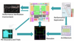
Where does NoC design start?
I’ve always wondered about where NoC design starts. Do you go for design for traffic optimization first, then floorplan, or the other way round? According to Sondrel either approach can take a while to converge. They start instead with architectural performance exploration. This is used to decide on an appropriate size for the interconnects and memory subsystem by modelling the memory traffic patterns that are generated by all the subsystems as if they were running on the real system (to a reasonable approximation). Here I believe they start with spreadsheet estimation, then move to SystemC modeling with channels for connectivity.
Once this step has converged, then they start running real trials on NoC RTL. This is generated to match the goals of the performance exploration. This they do using a proprietary testbench called Performance Verification Environment. The RTL connects to transactors modeling processors and subsystems defined in Python. In this flow Python generates memory-mapped bus traffic is generated and drives it through the NoC. Allowing the NoC architect to quickly see what is going on in the design and how changes will improve the data traffic flow.
In this flow, the NoC definition starts from an already converged architectural performance goal. From Sondrel’s perspective it is then much easier to fine tune the NoC for performance and floorplan deltas. Avoiding major oscillations in the plan. It is also easier to adjust the NoC architecture as needed in response to spec updates. Just as important, providing feedback to their customers on likely impact of those changes on key performance metrics.
SemiWiki has been tracking the popularity of chiplets for two years now so it was not surprising to see that they played a key role at DAC. The other trend we foresaw was that the ASIC companies would be early chiplet adopters and that has proven true. One of the more vocal proponents of chiplets at DAC#59 was OpenFive, a 17+ year spec-to-silicon design company with more than 350 tapeouts and more than 150M parts shipped, simply amazing!
Chiplets are all about reusability and quick time-to-market for chips big and small. Using silicon proven hard IP enables design starts by reducing costs and cutting tapeout time, which of course plays perfectly into the spec-to-design ASIC business perfectly.
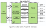
OpenFive has gained significant momentum in this trending market with several early customer engagements and multiple wins on D2D IP for chiplets. OpenFive also recently announced that they have joined the Universal Chiplet Interconnect Express (UCIe) Consortium which we covered (OpenFive Joins Universal Chiplet Interconnect Express (UCIe) Consortium). OpenFive is very well positioned based on their D2D IP, custom silicon implementation, and advanced packaging and manufacturing experience.
Features IOs running at up to 16Gbps (effective throughput of ~1.75Tbps/mm)
Features extremely low latency and <0.5pJ/bit offering best power performance benchmarks
It’s all about the ecosystem, right?
The new D2D PHY helps disaggregate large SoC die into smaller die, resulting in better yield, cost and power savings. It features up to 16Gbps NRZ signals with clock forwarding architecture. Each channel, comprising of 40 IOs, can provide effective throughput of up to ~1.75Tbps/mm. Users can stack up multiple channels to further increase overall throughput. The PHY also features built-in PLL, programmable output drivers, and link training state machines.
“The D2D subsystem, including both the controller and PHY, provides best-in-class latency, performance and power profile for various IO, CPU and analog chiplets,” said Ketan Mehta, Sr. Director, Product/Application Marketing, SoC IP, at OpenFive.
“OpenFive’s die-to-die connectivity IP solution will enable widespread integration of proven solutions from chiplet ecosystem partners,” said Mohit Gupta, SVP and GM, SoC IP at OpenFive. “As a custom ASIC and IP provider, OpenFive is well-positioned to provide an entire chiplet solution to our customers at any stage of development, whether it be during design, integration, manufacturing, or testing of Known-Good-Die (KGD).”
In their DAC booth OpenFive also highlighted an eye catching demo of an AI vision application and working silicon SoC boards which included:
About OpenFive
OpenFive, a SiFive business unit, is focused on custom silicon solutions and differentiated IP. With spec-to-silicon design capabilities, customizable SoC platforms, and differentiated IP for Artificial Intelligence, Cloud/Datacenter, High Performance Computing, Networking, and Storage applications, OpenFive is uniquely positioned to deliver highly competitive processor agnostic domain-specific SoCs.
The OpenFive IP portfolio includes High-Bandwidth Memory (HBM3/2E) and low power LPDDR5/4x memory subsystems; Die-to-Die (D2D) interface IP subsystems for heterogeneous multi-die connectivity including chiplets; low-latency, high-throughput Interlaken interface IP for chip-to-chip connectivity; 400/800G Ethernet MAC/PCS subsystems, and USB controller IP. OpenFive offers end-to-end expertise in custom SoC architecture, design implementation, software, silicon validation, and manufacturing to deliver high-quality silicon in advanced nodes down to 4nm.
Designing complex systems is difficult. It seems to me that the difficulty has increased at a rate that is more exponential than linear with design complexity. Some version of Moore’s law for design is at work. The challenges for advanced designs just seem to keep mounting. A new item that is top of mind for many executives is the talent shortage. Even if you had the budget, you just can’t find enough qualified engineers. It’s a vexing problem with many proposed solutions. At the root of many solutions is a simple, elegant focus – a solid methodology is the margin of victory.
Semifore recently posted a press release – CommScope Selects Semifore to Accelerate Product Development and Improve Quality of Results. This sounded like one of those margin of victory strategies. You can read the press release at the link provided. It’s also on Semifore’s SemiWiki page here, with lots of other good information about the company. In this post, I wanted to explore the story beyond what was in the press release. Does Semifore deliver a margin of victory strategy? Here is what I found.
Who is CommScope?
First, a bit about the company mentioned in the press release. According to the press release:
CommScope is a global leader in communications technology to create the world’s most advanced networks. Across the globe, the company is redefining connectivity, solving today’s communications challenges, and driving the innovation that will meet the needs of what’s next.
Networks and communications are indeed a critical enabler for a lot of what’s next. The company provides both hardware and software to enable broadband, enterprise and wireless networks. The product line, support strategy and overall focus on the big picture are quite impressive. After some digging, I wanted to learn more about how ambitious companies found the margin of victory in their markets, and how Semifore fit.
For that, I spoke with Semifore’s co-founder and CEO, Rich Weber. Rich has a storied career designing complex systems at major corporations such as Data General, Silicon Graphics and Cisco.
Exploring the Margin of Victory with Rich Weber
My conversation with Rich explored the bigger picture of what it takes to successfully build a complex system. The specifics for CommScope are outlined in the press release. I was after the bigger story.
Our discussion began with several stories of confusion and chaos. They all tied back to a lack of a solid methodology and timely communication. The stories Rich related were primarily focused on the hardware/software interface, or HSI for complex systems. The HSI is composed of many registers that implement the complex protocols allowing software to control the hardware required to implement the software algorithms.
Small errors in this part of the system can cause big problems. Beyond the visible failure mode of “it didn’t do what we expected” there is the invisible failure mode of “the new feature can’t be implemented because the HSI doesn’t seem to support it”. It turns out that errors in the HSI implementation aren’t the whole story. Rich described several scenarios where a well-meaning engineer made a seemingly harmless change to a bit in the HSI on a Friday evening. That caused regressions to fail over the weekend and further cause the data that was driving the various teams working on the project to be invalid. Teams like documentation, testing and design were all victims. Monday morning was met with chaos. The HSI is quite fragile – small tweaks can result in big headaches.
We also talked about specifying the HSI and the role standards play. It turns out Rich has been directly involved in developing many of these standards through organizations like Accellera. Standards such as SystemRDL and IP-XACT. What I discovered in my discussions was that these standards are certainly useful, but they all fall short of delivering a complete, robust solution that can express all aspects of the HSI. Solving this problem allows an executable specification of the HSI to be developed, something of a holy grail item for many design teams.
With this backdrop, I began to see a pattern. Semifore offers a way to fully specify the HSI with a robust language (the elusive executable spec). They also offer a way to create a correct-by-construction HSI with accurate, up-to-date representations for all team members. No more chaos.
It seems like CommScope figured out that a solid methodology is the margin of victory. If you dig into what Semifore is up to, you may find your margin of victory as well.
Tuesday at DAC I had the pleasure of attending the Design on Cloud Theatre where experts from Siemens EDA gave an update on what they’ve been offering to IC and systems designers. I remember attending a cloud presentation from Craig Johnson in 2021, so I was keen to note what had changed in the past 12 months.
Craig Johnson, Siemens EDA – VP Cloud Solutions
Industry Trends, Design on Cloud
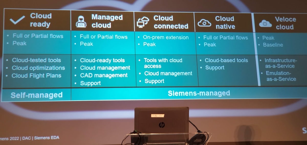
Craig shared that there’s been increased adoption over the past 5 years, abd more deployments of EDA design on cloud. Why? The improved throughput, cost, and security are all factors, and it depends on the goals of each team.
The EDA requirements have been unique per design team, due to the different size of projects, so no one cloud solution fits all EDA users. Siemens EDA has responded by offering a range of five cloud choices:
Cloud ready
Managed cloud
Cloud connected
Cloud native
Veloce cloud
Cloud choices
Craig had Brian Ramirez, from the Design Verification Technology group join him, then Brian shared some conclusions from the latest Wilson Research Group survey about biggest verification challenges:
1) Coverage closure
2) Isolate and fix bugs
3) Find the next bug
Verification, Design on Cloud
Brian Ramirez, Design Verification Technology
Reaching more verification requires more compute resources, and often that’s only available in the cloud, where teams can get more verification cycles quicker. Engineers can find and fix these verification challenges quicker in the cloud. Or, run more cycles to uncover more bugs.
Brian said that cloud users are seeing extreme peaks and valleys in their workloads , and that capacity was greater than licenses owned. There are often just too many options with so many cloud configurations, so that knowing what is the right balance to achieve cost and turn around times is a challenge.
There’s also some data overload, where too much time is spent to isolate and then resolve a bug. Verification engineers are spending most of their time just in debug, so how should we make the debug journey more efficient?
There are a lack of standards, as so many cloud suppliers create incompatible flows, so it’s not easy to move from one cloud provider to another one. What will solve these four issues?
Questa in the cloud can help, at a high scale, reaching up to a million hours in a day. Verification teams can maintain their workflows, be flexible, and not shoe horn into just one flow. Hybrid flows are offered in the cloud, with optimized cost, and faster time to closure. Functional verification questions, talk to Brian.
AMS Verification, Design on Cloud
At DAC 2021 I heard a presentation from Nebabie Kebebew on process variability, and this year at DAC she addressed the topic of AMS verification in the cloud. AMS flows have moved to the cloud, as they are often quite compute intensive, while on-premise verification can simply run out of steam, because of time. AMS workflows on the could are now supported, like circuit simulation with Analog FastSPICE.
Nebabie Kebebew. Senior Principal Product Engineer
With cloud simulation you can explore more, and actually meet PPA requirements. The cloud flight plans are provided by Siemens EDA, which are reference architectures for designers, and they have methodology white papers, and application notes to help AMS designers get started quickly. The flight plans are tuned per cloud provider. There are Analog FastSPICE papers for how to best use the cloud. There are many AMS tools from Siemens EDA, ready for cloud use, like: Eldo, Symphony, Solido Variation, Solido Characterization Suite.
Physical Verification
Michael White, from the Physical Verification Calibre team, noted that they have been using large-scale compute and cloud for about 15 years now. Internally they were using the cloud for EDA tool development, and now they are allowing customers to also use the cloud, so why consider using the cloud now for physical verification?
Michael White, Sr. Director
The compute requirement for DRC/LVS has exploded with smaller nodes – double patterning, multi patterning, EUV. EDA vendors have turned to the major cloud providers to enable EDA in the cloud: AWS, Google, MS Azure.
Examples of physical verification in the cloud include: Calibre PERC- reliability checking, Calibre DRC – design rule checking. Both of these EDA tools scale very well up to thousands of physical cores. The EDA technology must be cloud ready, optimized with foundry decks, and engineers must have the freedom to choose both their foundry and cloud vendors. There are reference architectures for each cloud vendor, so Siemens EDA is really taking a cloud vendor agnostic approach. Using cloud flight plans, with the best known methods, and even infrastructure as code for Calibre, you get a tailored experience for each cloud provider.
Systems, Design on Cloud
Craig introduced the next presenter, Paul Welch, from the Electronic Board Systems group. Paul sees that the typical boards and systems engineers are in industries, like: mil-aero, medical, automotive, IoT. These system flows are different than IC flows. For a systems design there is a BOM, the board is checked to be manufacturable, prototypes are built, and and engineer has to verify prototypes, finally they have to iterate the system and manufacture process again.
Paul Welch, Electronic Board Systems
For systems design the lead time, and number of iterations is too long, causing an over run of the budget. So this digital transformation is a challenge, namely how to realize the digital twin.
Boards are being designed in the cloud with several tools: Xpedition, HyperLynx, PADS Pro Premium. A new board design may start on the designers desktop, and then the supply chain is a challenge, because how does an engineer find parts from the supply chain?
The cloud approach delivers real time component insight on the desktop, along with cost, lifecycle management, predictive risk factors, and the early feedback to reduce supply chain risks. Parts not selected that are on back ordered can be dealt with. For collaboration a team member can choose to work from home, or work from anywhere, and there’s a cloud product called Connect for PADS Professional .
Cloud visualization using a web browser allows you to see the schematic, and layout, and BOM online, all without sending an email update to everyone else. Coming attractions: elastic compute around advanced packaging to solve challenges more quickly. Blockchain – trust and traceability in the supply chain, provenance of each part.
Consulting and Learning Services
The final presenter was Sam George, Consulting and Learning Services, and he started in the industry back in 2001 where they pioneered the hosted model. Yes, there were early doubts of feasibility for cloud design, but now it’s much easier with 3rd party cloud vendors, plus the applications are ready and cloud friendly, the engineers are accustomed to using cloud apps.
Sam George
The Managed Cloud is an approach where Siemens manages all of the IT aspects for a design team, and provides access to the cloud-based tools required. This is a full-flow, where a thin client accesses the cloud for schematic, PCB layout, analysis, plus interactive and batch tool usages.
With the Hybrid cloud where there are both peak and batch usages, the engineering team has their day to day workload on premise, but then uses cloud just for the peak licenses. This is making it easier to use tools and services, in just the way you want to work. Security is on the top of people’s mind, along with access to all the apps, and finally the cost of tools. Engineers want to get their job done, so cloud usage is a big deal, with both interactive and batch submissions being supported.
Smaller design teams may want all of their CAD tasks managed in the cloud to start with, and then learn how to manage cloud usage themself.
Emulation in the cloud enables faster and earlier SW development. HW-assisted verification allows a team to do concurrent SW development, using real power profiles. An emulation service allows lower costs to a team than ownership. Siemens configures the emulator to start out with, and then helps teams to be successful with emulation.
Other teams purchase or lease an emulator, but still want Siemens to host the cloud and perform any maintenance tasks. Prototyping is offered in the cloud too, just like emulation.
Summary
Siemens EDA has really started to build out a rather impressive suite of cloud flows for IC and systems . There are five levels of using the cloud now, so there’s a size that fits the culture and budget of your engineering team. The big picture goal of design on cloud is to speed up projects.
In cybersecurity circles, the elephant in the room is a quantum computer in the hands of nefarious actors. A day is coming, soon, when well-funded organizations will be able to rent time on, or maybe even build or buy a quantum machine. Then, if data is valuable enough, people will hunt for it. Two or three months of compute time on a quantum computer will break any asymmetric encryption algorithm (such as elliptic-curve and RSA) in any device that exists today. The longer devices with these dated asymmetric algorithms hang around, in some cases 10 or 15 years, the more vulnerable they get. But the game is changing with post-quantum cryptography stepping on the field, with new algorithms and hardware and software IP.
Six-year NIST competition pares down candidates
The U.S. Department of Commerce’s National Institute of Standards and Technology (NIST) began its search for quantum-resistant successors to methods defined in three cryptographic standards with a call for proposals in December 2016.
Currently, FIPS 186-4 defines encryption methods, NIST SP 800-56A deals with key establishment, and NIST SP 800-56B covers digital signatures. All these standards rely on various public key algorithms with pairs of very large numbers, which get much larger when multiplied together. These pairs are safely out of reach for even today’s supercomputers, but a quantum computer can find them in a reasonable amount of time. With a device’s pairs exposed, it becomes compromised since the algorithms are public.
For general encryption, such as accessing secure websites, CRYSTALS-Kyber is a clear winner in manageable key sizes and speed of operation. It uses structured lattice technology, with hyper-dimensional grids (tens of thousands of axes, or more) and long basis vectors making it very difficult to find a small coordinate in the grid.
For digital signatures, essential for digital transactions or signing documents, three algorithms won. CRYSTALS- Dilithium is the primary choice, with Falcon a second option for more compact signatures. Both also use structured lattices. A more compute-intensive algorithm, SPHINCS+, uses hash functions in an alternative approach.
PQShield teams helped define device-ready algorithms
These algorithms came from teaming arrangements of experts around the globe. We’re introducing PQShield to readers as a hardware and software IP company. Before their products arrived, they invested years of research into these four algorithms. A PQShield researcher is development leader and co-author of Falcon. The other three algorithms, CRYSTALS-Kyber, CRYSTALS-Dilithium, and SPHINCS+, are co-authored by a PQShield advisory board member.
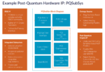
This first-hand insight is invaluable when putting complex algorithms into smaller, resource-bound devices. Anybody can run algorithms like these on a server. Realizing them in an SoC or a high-end microcontroller is another story. For post-quantum cryptography IP, PQShield developed its PQSubSys (short for Post Quantum Sub System), a co-designed, upgradable hardware/firmware coprocessor core.
Two options exist, one focusing on the post-quantum crypto IP elements shown within the dotted orange line above. PQShield can also provide a full solution shown within the blue line above including an entropy source, a RISC-V core and memory for an integrated cryptography subsystem. This integration leverages the Zkr Entropy Source extension PQShield defined as part of the RISC-V Scalar Cryptography Specification released in October 2021.
Giving SoC architects a new path forward
Before NIST announced its finalists, it would have been tough to give guidance to SoC architects. Building more devices with pre-quantum cryptography IP is far better than designing in no security, even knowing the vulnerabilities about to come. But now, the arrival of finalist post-quantum algorithms and optimized IP create a new path forward.
And soon, full-custom SoCs won’t be the only option for working with this IP. Microchip Technology has cut an IP licensing deal with PQShield, no product announced yet. Another clue is a new partnership between PQShield and Collins Aerospace, a long-time PolarFire SoC customer. The PolarFire SoC combines RISC-V cores with FPGA gates on one chip, and the PQShield IP seems like a fit there.
There’s still some work ahead on the details of post-quantum cryptography. Like any standards work, early adopters get a leg up but may have to withstand some minor changes between first and final versions. With algorithms and configurable IP in place, PQShield has the knowledge and tools chip designers need to create more secure devices.
For more info, PQShield is publishing their thoughts in an open newsletter:


