
In cybersecurity circles, the elephant in the room is a quantum computer in the hands of nefarious actors. A day is coming, soon, when well-funded organizations will be able to rent time on, or maybe even build or buy a quantum machine. Then, if data is valuable enough, people will hunt for it. Two or three months of compute time on a quantum computer will break any asymmetric encryption algorithm (such as elliptic-curve and RSA) in any device that exists today. The longer devices with these dated asymmetric algorithms hang around, in some cases 10 or 15 years, the more vulnerable they get. But the game is changing with post-quantum cryptography stepping on the field, with new algorithms and hardware and software IP.
Six-year NIST competition pares down candidates
The U.S. Department of Commerce’s National Institute of Standards and Technology (NIST) began its search for quantum-resistant successors to methods defined in three cryptographic standards with a call for proposals in December 2016.
Currently, FIPS 186-4 defines encryption methods, NIST SP 800-56A deals with key establishment, and NIST SP 800-56B covers digital signatures. All these standards rely on various public key algorithms with pairs of very large numbers, which get much larger when multiplied together. These pairs are safely out of reach for even today’s supercomputers, but a quantum computer can find them in a reasonable amount of time. With a device’s pairs exposed, it becomes compromised since the algorithms are public.
After several rounds of proposals, reviews, and revisions, on July 5th, 2022, NIST pared down the candidates to four algorithms:
- For general encryption, such as accessing secure websites, CRYSTALS-Kyber is a clear winner in manageable key sizes and speed of operation. It uses structured lattice technology, with hyper-dimensional grids (tens of thousands of axes, or more) and long basis vectors making it very difficult to find a small coordinate in the grid.
- For digital signatures, essential for digital transactions or signing documents, three algorithms won. CRYSTALS- Dilithium is the primary choice, with Falcon a second option for more compact signatures. Both also use structured lattices. A more compute-intensive algorithm, SPHINCS+, uses hash functions in an alternative approach.
PQShield teams helped define device-ready algorithms
These algorithms came from teaming arrangements of experts around the globe. We’re introducing PQShield to readers as a hardware and software IP company. Before their products arrived, they invested years of research into these four algorithms. A PQShield researcher is development leader and co-author of Falcon. The other three algorithms, CRYSTALS-Kyber, CRYSTALS-Dilithium, and SPHINCS+, are co-authored by a PQShield advisory board member.
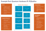
This first-hand insight is invaluable when putting complex algorithms into smaller, resource-bound devices. Anybody can run algorithms like these on a server. Realizing them in an SoC or a high-end microcontroller is another story. For post-quantum cryptography IP, PQShield developed its PQSubSys (short for Post Quantum Sub System), a co-designed, upgradable hardware/firmware coprocessor core.
Two options exist, one focusing on the post-quantum crypto IP elements shown within the dotted orange line above. PQShield can also provide a full solution shown within the blue line above including an entropy source, a RISC-V core and memory for an integrated cryptography subsystem. This integration leverages the Zkr Entropy Source extension PQShield defined as part of the RISC-V Scalar Cryptography Specification released in October 2021.
Giving SoC architects a new path forward
Before NIST announced its finalists, it would have been tough to give guidance to SoC architects. Building more devices with pre-quantum cryptography IP is far better than designing in no security, even knowing the vulnerabilities about to come. But now, the arrival of finalist post-quantum algorithms and optimized IP create a new path forward.
And soon, full-custom SoCs won’t be the only option for working with this IP. Microchip Technology has cut an IP licensing deal with PQShield, no product announced yet. Another clue is a new partnership between PQShield and Collins Aerospace, a long-time PolarFire SoC customer. The PolarFire SoC combines RISC-V cores with FPGA gates on one chip, and the PQShield IP seems like a fit there.
There’s still some work ahead on the details of post-quantum cryptography. Like any standards work, early adopters get a leg up but may have to withstand some minor changes between first and final versions. With algorithms and configurable IP in place, PQShield has the knowledge and tools chip designers need to create more secure devices.
For more info, PQShield is publishing their thoughts in an open newsletter:
PQShield Newsletter, July 2022
Also Read:
CEO Interviews: Dr Ali El Kaafarani of PQShield
NIST Standardizes PQShield Algorithms for International Post-Quantum Cryptography
WEBINAR: Secure messaging in a post-quantum world


