
Building a multi-FPGA prototype for SoC verification is complex with many interdependent parts – and is “always on a clock”. The best multi-FPGA prototype implementation is worthless if its not up and running early in the SoC design cycle, where it offers the highest verification ROI terms of minimizing the cost of bug fixes and accelerating the SoC time-to-market. So, any automation software that enables a more accurate, higher performing prototype implementation in less time should be warmly welcomed by the SoC verification people prototyping large SoCs.
There are at least three pertinent challenges to the implementation of multi-FPGA prototypes;
- Cutting large SoC designs into blocks that will “fit” into each FPGA of a multi-FPGA prototyping platform,
- Assuring the overall timing integrity of the multi-FPGA prototype when all the FPGAs are connected together, and
- Managing the trade-off between the scarcity of FPGA I/O pins that limits the amount of logic in a partition “cut” when the design is spread across several FPGAs, and the prototype performance.
Adding to these prototype implementation challenges are other second-order challenges, like connecting thousands of debug probes, which consumes FPGA connectivity and impacts utilization, and connections to real-world target systems, which consumes FPGA connectivity and FPGA I/O, that impact how easy, or difficult, it is to compile all the FPGAs into a multi-FPGA prototype in an acceptable amount of time with manageable effort. The tighter you pack the FPGAs (higher utilization), the harder it is for the FPGA compiler tools to find a place and route solution that meets timing targets, and the longer they will take to complete. But, we’ll defer discussion of these challenges to a future blog.
Automation tools for partitioning large SoC’s for multi-FPGA prototyping should offer a spectrum of “level-of-automation”, from heavily-assisted partitioning, where the user chooses to “guide” the partitioning process with specific design knowledge that will enable a specific partitioning result, to fully automatic partitioning, where the user kicks off a partition run and goes for coffee while the partitioner does its thing. The basis for choosing the level of automation may be as simple as project schedule, where the designer wants to get to a working multi-FPGA prototype in a hurry and is willing to sacrifice prototype performance for fast compile times. Some SoC designs lend themselves to intuitive partitioning across multiple FPGAs, and the partition “cut lines” are easily imagined by the designer, while other designers choose higher automation due to the complexity of the critical timing paths, or the prototype target performance, or an aggressive project schedule. Partitioning at the RTL level is great for early estimations of performance and prototype fit into a multi-FPGA hardware platform, while heavy designer involvement in partitioning may go straight to the gate-level and render unnecessary the need for RTL partitioning.
As unimaginable as it may be today, early commercial multi-FPGA prototyping products did not include integrated timing analysis. Correct prototype timing in the early days was achieved by applying input stimulus to the prototype and observing the prototype output waveforms with debug probes, and then manually adjusting the relative-edge timing of failed-timing paths by inserting additional FPGA logic gates into the failed-timing path to fix hold-time violations. That approach by FPGA prototype product providers quickly drew the wrath of early users and led to integrated timing analysis into the FPGA prototyping flow. Today’s complex multi-FPGA prototypes would be unmanageably difficult without system-level timing analysis that considers the prototype timing of multiplexed FPGA I/O pins, and interconnect cables between FPGAs.
The scarcity of FPGA I/O pins continues to be the bane of multi-FPGA prototyping, even with the new massively large prototyping FPGAs from Intel and Xilinx (up to 80M usable gates per FPGA), because the number of “natural partition cut” interconnections between SoC design partitions often far exceeds the available I/O pins on the FPGAs. The number of partition interconnections can number in the tens of thousands, whereas the number of available I.O pins on the latest prototyping FPGAs is only a few thousand (1,976 max single-ended HP I/O’s for the Xilinx VU19P, and 2,304 maximum user I/O pins for the Intel Stratix GX 10M. Consequently, multi-FPGA prototyping must often resort to pin-multiplexing the FPGA I/O pins to implement a multi-FPGA prototype. The pin-multiplexing is usually accomplished with TDM soft-IP that is implemented with FPGA logic gates with the embedded multiplexors run at the upper limit of the FPGA’s switching speeds. Different levels of pin-multiplexing (2:1, 4:1, etc.) effectively expands the effective FPGA I/O but sacrifices higher prototype performance.
So, it goes without saying that more automation for multi-FPGA prototype implementation is a good thing, and it comes as no surprise that S2C would offer more of a good thing to its customers by continuing to advance its multi-FPGA prototyping software. Hence, S2C has recently announced a new release of its Prodigy Player Pro-7TM prototyping software – for use with its Logic System and Logic Matrix families of multi-FPGA prototyping hardware platforms. S2C has been in production with these multi-FPGA hardware platforms now for a while that incorporate the largest available prototyping FPGAs, like the Xilinx VU19P and the Intel Stratix GX 10M.
According to S2C, the salient features of the new Player Pro-7 software include;
- RTL Partitioning and Module Replication to support Parallel Design Compilation and reduce Time-to-Implementation
- Pre/Post-Partition System-Level Timing Analysis for Increased Productivity
- SerDes TDM Mode for Optimal Multi-FPGA Partition Interconnect and Higher Prototype Performance
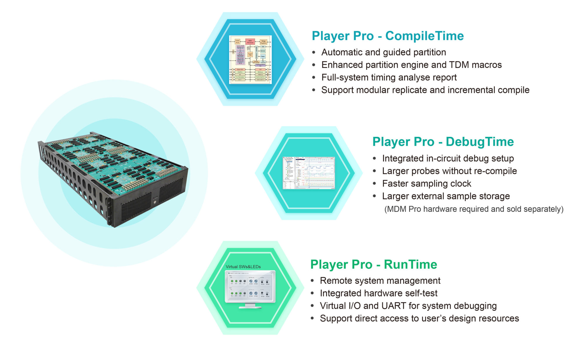
The new Player Pro-7 software suite is organized into three separate tools; Player Pro-CompileTimeTM, Player Pro-DebugTimeTM, and Player Pro-RuTimeTM. While the new releases of DebugTime and RunTime software include upgrades nfor multi-FPGA debug probing and trace viewing, and strengthening prototype hardware platform control and test, respectively – the most significant multi-FPGA prototyping feature improvements are in the new CompileTime software.

Previous releases of the Player Pro software supported design partitioning at the gate-level, so RTL partitioning is a big step forward for S2C, simplifying the management of multi-core design implementations, and enabling an early assessment of the number of prototype FPGAs required.
For more information about S2C’s multi-FPGA prototyping hardware and software, please visit S2C’s web site at www.s2cinc.com. Or, stop by S2C’s booth at the 2022 Design Automation Conference from July 11th to July 13th at the Moscone Center in San Francisco.
Also read:
Flexible prototyping for validation and firmware workflows
White Paper: Advanced SoC Debug with Multi-FPGA Prototyping
Prototype enables new synergy – how Artosyn helps their customers succeed
Share this post via:


Comments
One Reply to “Multi-FPGA Prototyping Software – Never Enough of a Good Thing”
You must register or log in to view/post comments.