I wrote last month about physically aware NoC design, so you shouldn’t be surprised that Arteris is now offering exactly that capability 😊. First, a quick recap on why physical awareness is important, especially below 16nm. Today, between the top level and subsystems a state-of-art SoC may contain anywhere from five to twenty NoCs, contributing 10-12% of silicon area. Interconnect must thread throughout the floor plan, adding to the complexity of meeting PPA goals in physical design. This requires a balancing act between NoC architecture, logical design and physical design, a task which until now has forced manual iteration, materially extending the implementation schedule. That iteration is a time sink which physically aware NoC design aims to cut dramatically.
(Source: Arteris, Inc.)
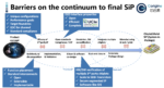
The Traditional Interconnect Design Flow
The early stages of NoC design are architecture-centric, figuring out how typical software use cases can best be supported. The network topology should be optimized around quality of service for high-traffic paths while allowing more flexibility for lower frequency and relatively latency-insensitive connections. Topology choices are also influenced by early floor plan estimates, packaging constraints, power management architecture, and safety and security considerations. Architects and NoC design teams iterate between an estimated floor plan and interconnect topology to converge on an approximate architecture. This planning phase consumes time (14-35 days in a production design example illustrated here), essential to approximately align between architecture, logic and physical constraints.
Then the hard work starts to refine approximations. System verification and logic verification are run to validate bandwidth and latency targets. Synthesis, place and route and timing analysis probe where the design must be further optimized to meet power, area and timing goals. At this stage, designers are working with a real physical floor plan for all the function IP components, into which NoC IPs and connections must fit. Inevitably, early approximations prove not to be quite right, the physical design team can’t meet the timing goals, and the process must iterate. Physical constraints may need to be tuned and pipelines added, driven by informed guesswork. More iterations follow further refining estimates and ultimately leading to closure. Sometimes fixing a problem may require a restart to refactor the NoC topology, putting the whole project at risk.
Those iterations take time. In one production design, closing NoC timing took 10 weeks! Experienced design teams limit iterations by over-provision pipelining and by using LVT libraries along timing critical paths. Accepting tradeoffs in area, latency and power in exchange for faster convergence. Per iteration, considering and implementing those decisions then rerunning the implementation flow and rechecking timing, altogether can take weeks.
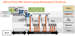
Physically Aware NoC Design With FlexNoC 5
That trial-and-error iteration is a consequence of approximations and assumptions in architectural design. Understandable but now a much better approach is possible. After the very first pass-through implementation, a more accurate floor plan is available. Maybe the NoC topology needs to be tweaked against the floor plan but now it is working with real physical and timing constraints. The NoC generator has enough information to generate more accurate timing and physical constraints for P&R. It can also insert the right level of pipelining, exactly where it is needed. Automatically delivering a NoC topology which will close with confidence in just one more implementation pass.
(Source: Arteris, Inc.)
This is what Arteris is claiming for their new generation FlexNoC 5 solution – that a first iteration based on an implementation grade floor plan will provide enough information for FlexNoC 5 to automatically generate timing and physical constraints, together with pipelining, to meet closure on the next pass. Based on the customer design example described earlier, they assert that this automation delivers up to a 5X speedup in iterating to NoC physical closure.
That’s a big jump in productivity and one that seems intuitively reasonable to me. I talked in my earlier blog about the whole process being an optimization problem with all the challenges of such problems. A trial-and-error search for a good starting point suffers from long cycle times through implementation, to determine if a trial missed the mark and how to best adjust for the next trial. More automation in NoC generation based on more accurate estimates should find an effective starting point faster.
Proving the Claim
Arteris cites measured improvements in NoC physical implementation using a FlexNoC 5 flow, in each case using the same number of engineers with and without the new technology. For pipeline insertion, they were able to reduce iterations from 10 to 1, within the same time per iteration. In constraint (re-) definition they were able to reduce the elapsed time from 3 days to 1 day and turns on constraints from 3 to 1. In place and route, they were able to reduce 5 or more iterations to 1 iteration within the same or better iteration time. Overall, 10X faster in pipeline insertion, 9X faster in constraint (re-)definition and 5X faster in P&R.
I should add that a customer in this case (Sondrel) has significant experience in ASIC design and has been working with NoC technology for many years. These are experienced SoC designers who know how to optimize their manual flow yet agree that the new automated flow is delivering better results faster.
You can learn more about FlexNoC 5 HERE and about Arteris HERE.