

My recent article, ‘Chip War without Soldiers’ explained the importance of upskilling and preparing the chip design workforce in this current scenario, and it also explained how it will lead to ‘Fabs without Chips’ if we don’t prioritize it. VLSI Engineers are the pillars of the semiconductor industry, and they can only transform our industry into a trillion-dollar industry with their inventions and innovations. So, in this article, I want to explain how Maven Silicon can collaborate with your organization as the VLSI Centre Of Excellence for upskilling your chip design workforce and why you should choose Maven Silicon as your preferred VLSI training partner.
To understand ‘Why Maven Silicon for upskilling your workforce?’ – Let me convince you with our USPs.
Maven Silicon USPs:
- Scalable Training Services: Maven Silicon is the only VLSI training company that can train engineers in bulk worldwide using our cloud-based online training solutions. We are the one who introduced this kind of innovative learning subscription model to tier-1 global product and services semiconductor MNCs. Today we train thousands of VLSI engineers every year for our enterprise customers. At Maven Silicon, we also provide ILT-Offline and VILT-Blended-online courses for project-specific specialized training courses. So, we can support your workforce L&D initiatives at any scale as per your business requirements.
- Flexible Business Models: We offer inexpensive multi-year learning subscription business models to upskill an army of engineers globally, along with our standard corporate training business models, which involve training a batch of engineers [Instructor-Led Offline Project/Domain specific Specialized Training] periodically for various projects.
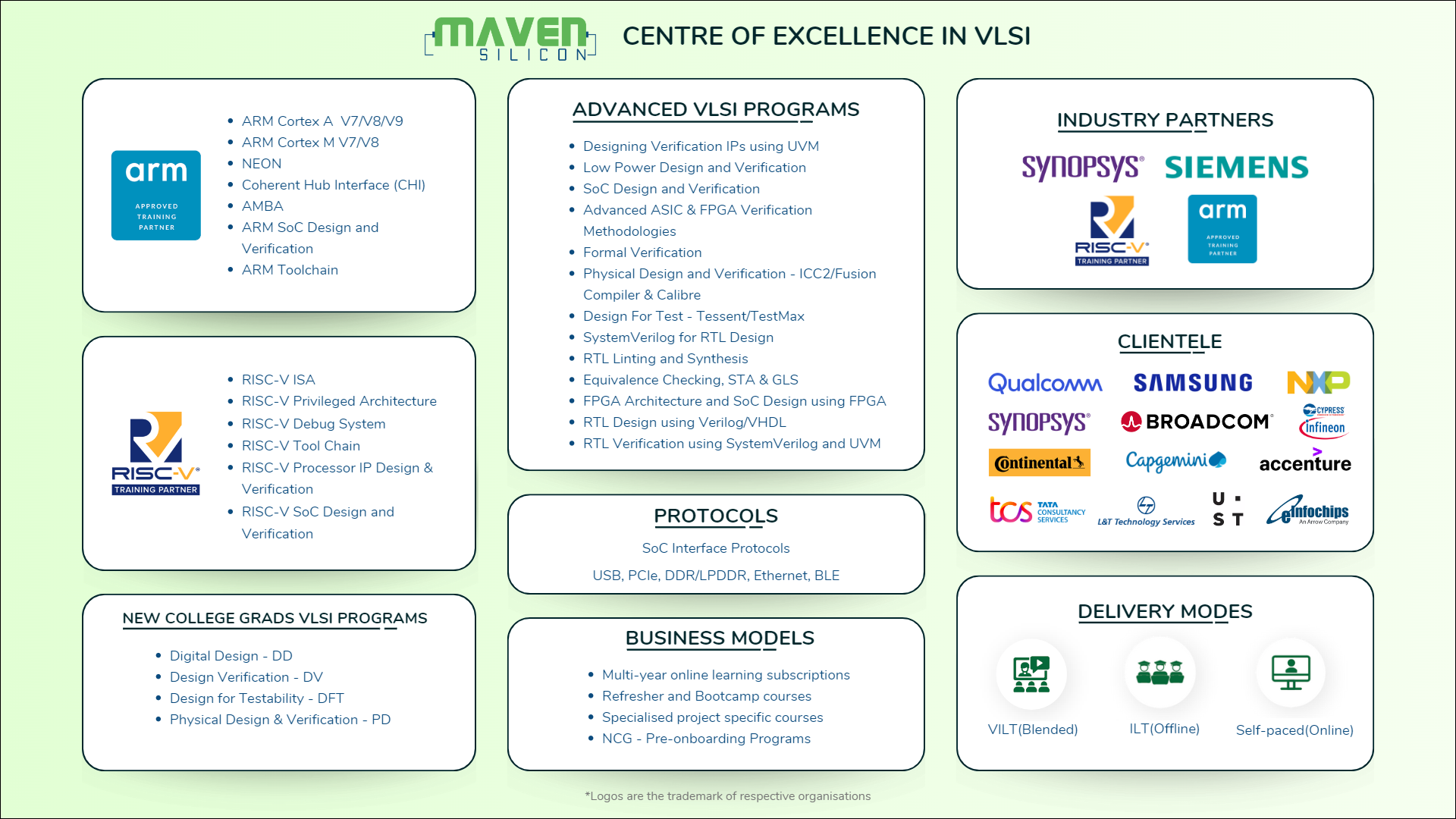
- Domain Expertise: Maven Silicon has been designated as ARM Approved Training Partner by ARM and Global RISC-V Training Partner by RISC-V International to train the VLSI engineers on their processor architectures. Synopsys and Siemens EDA are our EDA partners. All our lead trainers have been trained formally by our industry partners ARM, RISC-V, Synopsys, and Siemens EDA. Our trainers are specialized in various VLSI domains like RTL Design and Verification, DFT, Physical Design, SoC Design, ASIC & FPGA, ARM and RISC-V. The image below explains how we offer various VLSI courses and support our enterprise customers with our domain expertise and flexible business models.
Click here to view the full image
I also want to share some of the myths and fallacies about upskilling the VLSI engineers we observed while interacting with the project managers and business heads in India and explain how we can collaborate with your L&D team to address their challenges or concerns.
Myths & Fallacies:
1) Internal Training is very effective and inexpensive: Internal training might be effective, but it’s not a scalable model. Refer to our USPs 1&2. Involving your experienced and expensive project managers as trainers in the internal training programs will be more expensive than involving external vendors. Training services are our core business, so we deliver our courses efficiently with our unique pedagogy and curricula. We regularly learn new technologies and update our curricula.
A traditional, highly experienced project manager may not be competent to train the next generation of engineers on the latest technologies and design methodologies. For example, V-Plan based CRCDV using UVM is different from Test plan-based HDL verification. Some experienced traditional DV project managers refer to the Test plan [Directed testcases] while using UVM/SystemVerilog, like how we casually use the term ‘DUT’ for DUV. Can they quickly unlearn traditional and outdated techniques/methodologies? What if they leave your company because of this additional training responsibility – teaching, developing, and maintaining course content? What about the additional efforts and expenses incurred by your LMS software and EDA licenses? What is your core business – EDA or Product or Design Services, and why don’t you dedicate your expensive, experienced resources to grow your core business?
2) External Training is expensive: Why should a billion-dollar VLSI company be conservative as miserliness for upskilling its workforce? It’s time for us to think beyond free learning subscriptions and internal training programs and invest more in new L&D initiatives to support our VLSI engineers for their long-term career development. Refer to our USPs 1&2. We offer various online and offline VLSI training programs with flexible business models to upskill your engineers efficiently within your L&D budget. Companies that support engineers generously for their long-term career growth can retain them for long and grow them as next-generation leaders. Hiring culturally fit experienced engineers, project leads, managers, architects, and engineering directors from competitors is very expensive than investing in L&D upskilling initiatives. Isn’t it?
3) Internship is more effective than direct hiring: Whether direct hiring or internship, it can be more effective only with proper training and coaching/mentorship. In the case of hiring New College Graduates, we partner with our customers to upskill them using our pre-onboarding NCG training courses. It is unique as this pre-onboarding training begins during their engineering course during the pre-final/final year. It works beautifully for the companies to onboard them efficiently without much attrition. Most electronics/electrical engineers are still attracted to the software giants because of the lucrative career and complexity of the VLSI technology. Formally upskilling passionate engineers can help them to deal with VLSI comfortably. So, they will choose our industry and pursue their long-term VLSI career. The internship is more effective with our pre-onboarding training, and it reduces the duration and cost of the internship minimum of 50% for the company. Why do you still want to follow the same informal/traditional on-the-project internship/training? Is it effective?
We can dream about transforming our semiconductor industry into a trillion-dollar industry only with creative and skilled chip design engineers. We need next-gen advanced node chips to implement and support new technologies like AI, 5G, Cloud, etc., and grow our business. We need more creative and skilled engineers for the same. Are we gearing up with the next generation of skilled chip designers to design more new chips, especially working chips, and make the fabs busy?


