The point spread function is the basic metric defining the resolution of an optical system [1]. A focused spot will have a diameter defined by the Airy disk [2], which is itself a part of the diffraction pattern, based on a Bessel function of the 1st kind and 1st order J1(x), with x being a normalized coordinate defined by pi*radius/(0.5 wavelength/NA), with NA being the numerical aperture of the system. The intensity is proportional to the square of 2J1(x)/x. The intensity profile is the point spread function, since it is the smallest possible defined pattern that can be focused by a lens (or mirror). The full-width at half-maximum (FWHM) is closely estimated by 0.5 wavelength/NA. DUV patterns are often much smaller than this size (down to ~0.3 wavelength/NA) and are thus required to be dense arrays and use phase-shifting masks [3].
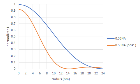
In the context of EUV lithography, there are 0.33 NA systems and 0.55 NA systems with 20% central obscuration. The latter requires a modification of the point spread function by subtracting the point spread function corresponding to the obscured portion. For a 20% central obscuration, this means subtracting 0.4 J1(0.2x)/x, i.e., the intensity is proportional to the square of [2J1(x)/x – 0.4 J(0.2x)/x]. The point spread functions for 0.33 NA and 0.55 NA EUV systems are plotted below.

The 0.55 NA system has a narrower FWHM, ~12.5 nm vs ~21 nm for 0.33 NA. However, the larger NA goes out of focus faster for a given defocus distance due to larger center-to-edge optical path differences [4]. Moreover, experimentally measured EUV point spread functions [5] indicated much reduced contrast than expected from a ~22 nm FWHM point spread function for a 13.5 nm wavelength 0.3 NA system. This can be attributed to aberrations but also significantly includes relatively long-range effects specific to the resist, which can be attributed to photoelectrons and secondary electrons resulting from EUV absorption [6].
As indicated earlier, spot sizes smaller than the point spread function are possible only for dense pitches, with a lower pitch limit of 0.7 wavelength/NA. For random logic arrangements on interconnects, however, pitches have to be much larger, and so line cuts, for example, are still limited by the point spread function. On current 0.33 NA EUV systems, for example, it can be seen that the point spread function already covers popularly targeted line pitches in the 28-36 nm range. So, in fact, the edge placement from overlay and CD targeting, compounded by the spread of the secondary electrons [6,7], looks prohibitive. No wonder, then, that SALELE (Self-Aligned Litho-Etch-Litho-Etch) has been the default technique, even for EUV [8-11].
References
[1] https://en.wikipedia.org/wiki/Point_spread_function
[2] https://en.wikipedia.org/wiki/Airy_disk
[3] Y-T. Chen et al., Proc. SPIE 5853 (2005).
[4] A Simple Model for Sharpness in Digital Cameras – Defocus, https://www.strollswithmydog.com/a-simple-model-for-sharpness-in-digital-cameras-defocus/
[5] J. P. Cain, P. Naulleau, and C. Spanos, Proc. SPIE 5751 (2005).
[6] Y. Kandel et al., Proc. SPIE 10143, 101430B (2017).
[7] F. Chen, Secondary Electron Blur Randomness as the Origin of EUV Stochastic Defects, https://www.linkedin.com/pulse/secondary-electron-blur-randomness-origin-euv-stochastic-chen
[8] F. Chen, SALELE Double Patterning for 7nm and 5nm Nodes, https://www.linkedin.com/pulse/salele-double-patterning-7nm-5nm-nodes-frederick-chen
[9] R. Venkatesan et al., Proc. SPIE 12292, 1229202 (2022).
[10] Q. Lin et al. Proc. SPIE 11327, 113270X (2020).
[11] Y. Drissi et al., “SALELE process from theory to fabrication,” Proc. SPIE 10962, 109620V (2019).
This article first appeared in LinkedIn Pulse: Lithography Resolution Limits: The Point Spread Function
Also Read:
Resolution vs. Die Size Tradeoff Due to EUV Pupil Rotation
Multiple Monopole Exposures: The Correct Way to Tame Aberrations in EUV Lithography?
Application-Specific Lithography: Sub-0.0013 um2 DRAM Storage Node Patterning
Share this post via:


Solving the EDA tool fragmentation crisis