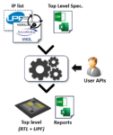
In the world of semiconductor design, constraints are essentially specifications and requirements that guide the implementation of a specific hardware or software component within a larger system. They dictate timing, area, power, performance, and of course functionality of a design, playing a crucial role in ensuring that the design meets its intended objectives. There are also system-level constraints that address requirements and specifications at a broader level, encompassing the entire system or a collection of interconnected components.
As such, applying constraints accurately at various levels of the design hierarchy is essential, whether it is an IP block or a complete SoC that is being designed. At the same time, this process poses significant challenges, particularly across different levels of a complex design hierarchy. As design specifications evolve and intricate IP blocks are integrated into System-on-Chip (SoC) designs, the intricacies of timing, power, and area constraints become tricky. The manual management of this process is highly error-prone, often resulting in inconsistencies and conflicts that may go undetected until later stages of the design cycle.
Additionally, as a design evolves, constraints are refined to meet performance targets, introducing further complexities. The need for precision in propagating constraints from the system level to IP blocks, coupled with the dynamic nature of design iterations, underscores the importance of automated tools and methodologies. Automated constraint management becomes a critical enabler for achieving design predictability, reliability, and ultimately, successful tape-outs. An automated constraints promotion (ACP) methodology not only streamlines the constraint extraction, mapping, and propagation processes but also contributes to error reduction, ensuring that constraints remain accurate and coherent throughout the design evolution.
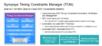
Synopsys recently hosted a webinar to address the topic of timing constraints management, covering the ACP methodology in the context of utilizing Synopsys Timing Constraints Manager. The webinar closed with the presentation of results from a case study that focused on early release PCIe® Gen6 subsystem timing constraints management.
Synopsys Timing Constraints Manager (TCM) Tool
Synopsys TCM empowers designers with a visual inspection and review capability for promoted constraints, offering a clear representation of their application across various levels of the design hierarchy. This feature facilitates a comprehensive understanding of how constraints are influencing different aspects of the design. Furthermore, TCM’s integration with verification tools plays a critical role in ensuring the accuracy and alignment of promoted constraints with the design intent and specifications. Thorough verification is facilitated through this integration, providing design teams with the confidence that the constraints are in line with the project’s requirements.
Key aspects of TCM’s value proposition include dedicated flows for constraints verification, promotion, and demotion, ensuring constraint integrity across different design hierarchy levels. Equally important is its scalability, catering to diverse IPs and configurations, making it adaptable to the varied complexities of semiconductor projects. TCM’s automation capabilities contribute to a notable turnaround time, reducing constraint-related activities from weeks to days without compromising the integrity of IP constraint reuse.
QuickStart Implementation Kits (QIKs)
Complementing TCM’s capabilities, the Fusion QuickStart Implementation Kits (QIKs) enhance productivity for design teams using Synopsys Fusion Compiler™, providing a swift start with tailored automation features. Fusion QIKs play a pivotal role in expediting the design process by providing designers with a valuable starting point. Specifically, these kits come equipped with pre-configured constraints, offering a consistent and reliable foundation for design teams embarking on their projects. This jumpstart proves invaluable especially when dealing with intricate designs such as a PCIe Gen 6 subsystem.
Furthermore, Fusion QIKs contribute to the efficiency of the design flow by simplifying the process of viewing and verifying results. Designers can leverage these kits to visualize and inspect results effectively, ensuring that the promoted constraints align with the design intent. This visualization step is crucial for designers to verify the accuracy and coherence of constraints, providing insights at the early stages of the design process and allowing for prompt identification and resolution of any potential issues. Ultimately, Fusion QIKs serve as a valuable tool in enhancing both the speed and reliability of the design process, ensuring a solid foundation for subsequent stages in the semiconductor design workflow.
The Benefits of the TCM/QIK Combo
The integration of TCM, coupled with the strategic use of Fusion QIKs increases the efficiency and accuracy of the design process. This is particularly crucial when dealing with high-speed and complex designs such as PCIe Gen 6 subsystems. The emphasis on early constraint promotion becomes a cornerstone for achieving enhanced design predictability and meeting the demanding timing requirements inherent in intricate designs. The above benefits were corroborated during a case study centered around an early release PCIe Gen6 subsystem configuration. The study spotlighted the critical importance of precise and early constraint promotion at the outset of the design process. Leveraging the Synopsys TCM tool enabled designers to not only address timing constraints but also to identify optimization opportunities related to power and area constraints specific to the PCIe Gen 6 subsystem.
Summary
Synopsys TCM helps streamline the creation and management of timing constraints for subsystems and System-on-Chips (SoCs), mitigating the challenges associated with manual approaches. TCM offers a comprehensive suite of functionalities, covering the entire spectrum from creation and verification to promotion, demotion, and equivalence checking. By adopting Synopsys’ tools and methodologies, design teams can navigate the challenges of the design process more effectively, contributing to successful outcomes in the development of advanced semiconductor products and electronics systems.
For more details, visit the Synopsys Timing Constraints Manager product page.
To listen to the webinar, watch on-demand here.
Also Read:
Synopsys.ai Ups the AI Ante with Copilot
Synopsys 224G SerDes IP’s Extensive Ecosystem Interoperability