You are currently viewing SemiWiki as a guest which gives you limited access to the site. To view blog comments and experience other SemiWiki features you must be a registered member. Registration is fast, simple, and absolutely free so please, join our community today!
When I first saw the Silicon Catalyst business plan 10 years ago I had very high hopes. Silicon Valley design starts were falling and Venture Capital Firms were distracted by software companies even though without silicon there would be no software.
Silicon Catalyst is an organization focused on accelerating silicon-based startups. It provides a unique incubation ecosystem designed to help semiconductor-centric startups overcome the challenges they face in bringing their innovations to market. Silicon Catalyst offers access to a broad range of resources including mentors, industry partners, investors, and other support services critical for the success of startups in the semiconductor space. The organization aims to foster innovation and entrepreneurship within the semiconductor industry by providing startups with the guidance, resources, and networking opportunities they need to thrive.
We have been collaborating with Silicon Catalyst for 4 years with great success. SemiWiki is part of the Silicon Catalyst ecosystem. We not only offer the incubating companies coverage (CEO interviews and podcasts), we attend the Silicon Catalsyt events and participate on many different levels. It has been an incredibly enriching partnership, absolutely.
One of the advantages of being a semiconductor professional is we get to work with the smartest and most driven people in the world. We also get to see new technologies developing that may change the world. I was on the ground floor of the smartphone revolution which changed the world and it does not even compare to what AI will do, my opinion. Bottom line: If you look at the Silicon Catalyst incubate companies you will see the future.
Two years ago Silicon Catalyst invaded the UK under the guidance of Sean Redmond. Sean and I started in Semiconductors the same year and have run into each other quite a few times, twice during acquisitions. Sean is the Silicon Catalyst Managing Partner for the UK. With the overwhelming success of the first one, Sean is launching the 2nd Cohort of the ChipStart UK Incubator. In the first cohort, eleven semiconductor startups are now half way through the nine month incubation with great success. They have full access to everything they need to deliver a full tape-out and experienced advisors to get them there safely.
I had a long conversation with Sean last week to get more details on semiconductors in the UK. AI seems to be driving the semiconductor community in the UK, and the rest of the world for that matter. Millions of dollars have already been raised by the first Chip Start program and Sean expects bigger things the second time around. The goal in the UK is to have a herd of semiconductor unicorns and I have no doubt that will be the case since the UK already has the 4th largest semiconductor based R&D.
Low power AI is a big part of the semiconductor push in the UK as you might suspect. Some of the applicants are spin outs from Universities and have first time senior executives. As part of the program classes are offered on IP strategy, legal protection, all parts of goto market plans, and of course fundraising. Exit strategies are also important as semiconductor start-ups have an average ten year life span so it is a marathon not a sprint.
Sean also mentioned that the GSA will return to the UK with an event in London next month in partnership with UK Government’s Department for Science, Innovation & Technology (DSIT) to jointly explore the impact of semiconductor innovation in anticipation to a NetZero economy. You can get details here:
Silicon Catalyst is the world’s only incubator focused exclusively on accelerating semiconductor solutions, built on a comprehensive coalition of in-kind and strategic partners to dramatically reduce the cost and complexity of development. More than 1000 startup companies worldwide have engaged with Silicon Catalyst and the company has admitted over 100 exciting companies. With a world-class network of mentors to advise startups, Silicon Catalyst is helping new semiconductor companies address the challenges in moving from idea to realization. The incubator/accelerator supplies startups with access to design tools, silicon devices, networking, and a path to funding, banking and marketing acumen to successfully launch and grow their companies’ novel technology solutions. Over the past eight years, the Silicon Catalyst model has proven to dramatically accelerate a startup’s trajectory while at the same time de-risking the equation for investors. Silicon Catalyst has been named the Semiconductor Review’s 2021 Top-10 Solutions Company award winner.
The Silicon Catalyst Angels was established in July 2019 as a separate organization to provide access to seed and Series A funding for Silicon Catalyst portfolio companies. SiliconCatalyst.UK. a subsidiary of Silicon Catalyst, was selected by the UK government to manage ChipStart UK, an early-stage semiconductor incubator funded by the UK government.
The relentless demand for lower power SoCs is evident across many markets. Examples include cutting-edge mobile, IoT, and wearable devices along with the high compute demands for AI and 5G/6G communications. Drivers for low power include battery life, thermal management and, for high compute applications, the overall cost of operation. Several approaches are available to achieve low power. A common thread for many is the need for optimal Foundation IP, that is, embedded memories and logic libraries. This is an area of significant investment and market leadership for Synopsys. Two informative publications are now available to help you understand the options and benefits that are available. It turns out achieving extreme low power with Synopsys Foundation IP memory compilers and logic libraries is within reach.
Let’s look at the information that is available.
Technical Bulletin
I’ll start with Optimizing PPA for HPC & AI Applications with Synopsys Foundation IP, a technical bulletin that focuses on logic libraries. The piece provides details on Synopsys’ tool-aware Foundation IP solution. Topics such as optimized circuitry, broad operating voltage range support and the flexibility to add customer-specific optimizations are discussed. The article also offers a perspective on achieving either maximum possible performance or the best power-performance trade-off. The figure below summarizes the logic library circuits available in the HPC Design Kit.
Synopsys HPC Design Kit components
Details of how power improvements are achieved is provided across many applications and design strategies. Topics that are covered include dynamic voltage scaling across a wide operating voltage range, optimizing AI and application-specific accelerator block PPA, solutions for network on chip, and how the Synopsys HPC Design Kit is co-optimized with Synopsys EDA for efficient SoC Implementation.
Also available is a comprehensive white paper entitled, How Low Can You Go? Pushing the Limits of Transistors. This piece digs into both embedded memories and logic libraries. It examines the details behind achieving extreme low power. Several application areas are discussed, including mobile, Bluetooth and IoT, high-performance computing, automotive, and crypto.
For embedded memories, several approaches are discussed, including assist techniques and splitting supply voltages. It is pointed out that careful co-optimization between technology and the design of memory assist circuits is required to deliver dense, low-power memory operation at low voltages. Several enhanced assist techniques are reviewed. Improvements in power range from 10% to 37%.
Reliability of memories is also discussed. The piece explains that as the voltage is reduced, the SRAM cell starts showing degradation. This degradation can cause multiple issues: reads are upset, the bitcell does not flip, SER is pronounced, sensing fails, control signals deviate, and the BL signal weakens. Therefore, assist techniques are needed to support the lower extreme low voltages required by cutting-edge low power applications.
The approaches Synopsys takes here make a significant difference. Strategies to improve reliability and methods to simulate aging are discussed. You should read the details for yourself – a link is coming. The data shows compelling results, with five to ten years of life added.
Logic libraries are also discussed, with strategies to enable deep low voltage operation at 0.4v and below. Architectural optimization is also reviewed. Standard cell architectural techniques can be employed to reduce both dynamic and leakage power. For example, Synopsys uses stack-based versus stage-based architectural techniques for the optimal topology for deep low voltage operation. The strategy behind this approach is presented.
Characterization optimization is also covered. One important piece of characterization is modeling process variation across an SoC, referred to as on chip variation (OCV). Several advanced techniques are employed here, including machine learning to increase accuracy and optimize performance and power.
The white paper concludes with an overview of how to put everything together at the SoC level to achieve deep low voltage operation. Voltage reduction is discussed, along with dynamic voltage and frequency scaling (DVFS) techniques and various shut-down strategies such as light sleep, deep sleep, full shut down and POFF (Periphery OFF) modes.
This white paper covers a number of power optimization topics in excellent detail. I highly recommend it. You can get your copy here. And that’s how achieving extreme low power with Synopsys Foundation IP memory compilers and logic libraries is within reach.
In the relentless pursuit of ever-increasing data speeds, the 1.6 Terabits per second (Tbps) era looms on the horizon, promising unprecedented levels of connectivity and bandwidth within data centers. As data-intensive applications proliferate and the demand for real-time processing escalates, the need for robust and efficient communication infrastructure becomes paramount. At the heart of this infrastructure lie electro-optical interconnects, poised to revolutionize data transmission with their blend of high-speed, low-latency, and power-efficient capabilities. The adoption of 224G serial links emerges as a critical enabler for achieving end-to-end 1.6Tbps traffic capacity. These high-speed serial links serve as the backbone of data transmission, facilitating seamless communication between various components within the network. Their ability to handle ultra-high data rates and bandwidth demands makes them indispensable for the realization of next-generation communication systems. As with every major technology advancement, there are inherent challenges to be overcome. Both the optical channel and optical engine introduce nonlinear behavior. Traditional simulation-assisted design methods often model optical engines using electrical circuit languages and simulators, assuming linear channels, leading to overly optimistic assessments of interconnect performance.
At the recently held DesignCon 2024 conference, Synopsys presented the results from their electrical-optical co-simulation study using native electrical and optical signal representations. A highlight of this study is that the system design methodology that was utilized accounts for both linear and non-linear impairments, agnostic of technology, data rate, and modulation format. The “System design methodology, simulation and silicon validation of a 224Gbps Serial Link” paper submission received DesignCon 2024 Best Paper Award.
The following are some excerpts from Synopsys’ two paper submissions at DesignCon, namely, “Performance assessment for high-speed 112G/224G SerDes with Direct-Drive Optical Engine” and “System Design Methodology, simulation and silicon validation of a 224Gbps serial link.”
Forward Error Correction in the 1.6T Era
Forward Error Correction (FEC) mechanisms play a pivotal role in enhancing the reliability of data transmission over high-speed links, particularly in the context of 1.6Tbps traffic. While FEC helps combat errors and ensures data integrity, its implementation introduces additional considerations such as power consumption and latency. Striking the right balance between Bit Error Rate (BER), power efficiency, and latency becomes imperative in designing efficient communication systems for the 1.6T era.
The Emergence of Electro-Optical Interfaces
To meet the evolving demands of the 1.6Tbps era, electro-optical interfaces are poised to play a transformative role. These interfaces leverage the advantages of optical technology to deliver high-speed, low-latency, and power-efficient communication solutions. Technologies such as Co-packaged Optics (CPO) and Die-to-Die (D2D) interconnects offer promising avenues for seamlessly integrating optical components into existing data center architectures, ushering in a new era of efficiency and performance.
Navigating Impairments in End-to-End Links
However, the deployment of end-to-end 224G links is not without its challenges. The conventional approach to simulating optical interconnects using electrical circuit languages and simulators, while effective in some cases, comes with several tradeoffs. Impairments such as noise, jitter, distortion, and crosstalk can significantly degrade signal quality and impact overall performance. To address these challenges, meticulous attention must be paid to modeling and mitigating impairments, ensuring the robustness and reliability of communication infrastructure in the face of non-linear effects inherent in optical and electro-optical interfaces.
The Role of Accurate System Modeling
Accurate system modeling is paramount in navigating the complexities of electro-optical interconnects and countering the non-linear effects inherent in optical transmission. By meticulously simulating various components and their interactions, designers can gain invaluable insights into system behavior and identify potential areas for optimization. Furthermore, correlation with silicon implementation ensures that simulation results closely align with real-world performance, enabling informed decision-making and efficient design iterations.
System Simulation to Silicon Correlation Comparison
In Synopsys’ electro-optical co-simulation study, the process of correlating system simulation with silicon involved a detailed setup for performance characterization in the lab. The setup encompassed various components including a BERT, cables, test board daughter card, and the device under test residing in an Ironwood socket. The s-parameters considered in the system model included responses from the Wildriver, the taconic fastrise 12-layer daughter card, and the testchip package. The comparison between silicon results and system simulation outputs showcased the correlation between the two. Overall, the findings from the study underscored the effectiveness of the system simulation model in capturing silicon behavior and provided valuable insights into system performance and optimization.
The below four charts indicate similarities in the PAM4 levels, EYE opening, and BER performance when simulation and silicon were compared.
The impulse response comparison below shows a slight difference in the lock point between simulation and silicon but overall correlation in shape.
The below chart shows the equalization capability of the receiver, with the DSP compensating for ISI and flattening the overall channel response.
The below chart captures the FFE and DFE coefficients from simulation and silicon readings, indicating some differences attributed to variations in the AFE transfer function and CDR lock point.
Summary
As data centers transition into the 1.6Tbps era, the integration of electro-optical interconnects holds the key to unlocking unprecedented levels of connectivity, bandwidth, and efficiency. Through meticulous system modeling, simulation, and correlation with silicon implementation, designers can harness the full potential of these technologies, ushering in a new era of innovation and performance in data center infrastructure. With the convergence of high-speed serial links, advanced FEC mechanisms, and emerging electro-optical interfaces, data centers are poised to meet the escalating demands of modern computing and networking applications, paving the way for a future of unprecedented connectivity and efficiency.
For more details and access to the full papers presented at DesignCon, please contact Synopsys.
After owning general purpose compute in cell phones and IoT devices, it wasn’t clear what Arm’s next act might be. Seemingly the x86 giants dominated in datacenters and auguries suggested a bloody war in smaller platforms between Arm and RISC-V. But Arm knew what they were doing all along, growing upwards into infrastructure: cloud compute, wired and wireless communications, out to gateways and even edge devices. At first modestly, recently more aggressively displacing mainstream processors and FPGAs as the front end to AI-centric GPUs, in hyperscaler scale-out and DPUs, in Telcos for gateways and wireless baseband, at the edge in automotive among other applications. To my mind this is an under-appreciated stealth invasion of the fast growing and high value infrastructure underpinning all of our electronic tech.
Consider
Take the Nvidia superchip – the one that propelled the company to a trillion-dollar valuation. This device, called Grace-Hopper, is actually 2 chips. Hopper is the GPU handling all the fancy AI stuff (tensor operations and such) and Grace is a CPU, very tightly coupled to Hopper and designed to handle the bridge to the regular cloud world through I/O and memory management functions. Grace is built on 72 cores of Neoverse V2. As for market value, witness the recent rise in Arm valuation, ascribed to “anything connected to AI”.
Amazon Web Services (AWS) build their power efficient Graviton scale-out servers, most recently their Graviton 4, on Neoverse. Demand for these platforms is high judging by the fact that almost of the AWS EC2 instances are based on Graviton rather than x86 processors. AWS also build their own machine learning platform (Tranium) which Arm cite in their slides, so I’m guessing that has a Neoverse front-end also.
Similarly, Microsoft have announced their Cobalt 100 server chip and their Maia 100 AI chip, both also cited in the Arm Neoverse slides and explicitly said be built on Neoverse. Note that between them AWS and Microsoft Azure own most cloud provider services (CPS) business by a wide margin. Notable also is that other CPS ventures are following similar paths.
Meanwhile, Nvidia have built their Bluefield DPU platform, AWS their Nitro hypervisor system and Microsoft their Azure Boost system, all around Neoverse. Neoverse is appearing all over the place in datacenters. They are already established in Ampere servers and in wireless infrastructure with Nokia, Ericsson and Huawei.
The Engine Driving Neoverse
Arm continues its tempo of new core introductions each year, this year adding V3 in the performance-optimized V-series, N3 in the performance/watt N-series and E3 in the data throughput E-series. Impressively the V2 (previous generation) already benchmarks ahead of X86 processors in SQL database performance, Java and XGBoost (the hot gradient optimizer for machine learning). V3 shows double digit advances over V2 in a range of enterprise-centric benchmarks and a whopping 84% advantage over V2 in AI data analytics. N3 equally shows impressive performance advances over N2 across the board and nearly 200% in AI data analytics.
A recent strategic move builds on Arm’s Compute Subsystem (CSS) cores, announced for the N-series in mid 2023. The previous generation CSS, as Arm describes it, is a customizable compute subsystem, verified, validated, and PPA-optimized by Arm. Think of a multi-core cluster objective for which you don’t just get the Lego pieces (CPU core, coherent interconnect, memory subsystem, etc.) but a complete customizable compute subsystem configured with Neoverse CPU cores, multiple DDR/LPDDR channels, multiple PCIe/CXL PHY/controller. All tuned, verified, validated, and PPA-optimized by Arm to client workloads and a target foundry/process through Arm’s Total Design program.
In this latest announcement, Arm have just announced a new CSS N3 configured to support from 8 to 32 cores per die running at as low as 40W thermal design power for 32 cores. They have also just announced their first V-series CSS, CSS-V3, providing 50% performance boost over CSS-N2. The Microsoft Cobalt chip is built on CSS-N2.
Given fierce competition between CSPs, mobile network operators, and auto OEMS (as an edge example) it seems clear that a diminishing number of product teams will see value in reinventing this CSS wheel themselves. From a CSP perspective, an opportunity to get compute subsystems tuned to their workloads, while saving development cost and time to market, yet preserving differentiated advantage seems like a no-brainer.
What About Software?
Arm is already tied into a well-established ecosystem at all layers of the software stack. For cloud applications it is especially important that Arm be closely tied to cloud-native activities in open-source leadership in languages, tools, Linux distributions, networking, etc., etc. Together with increasingly ubiquitous Arm-based instance, cloud-based software developers see obvious advantages not only to use Arm for development but also to preferentially offer those service on Arm platforms – a virtuous cycle.
To underscore that this strategy is working, Oracle now offer their 19C database platform supporting Arm-based hardware, both in the cloud and on-prem. Similarly, SAP has ported their SAP HANA cloud to AWS Graviton processors. Those are two giant enterprise applications. Given costs and software availability advantages, I am sure more software and SaaS providers will follow.
Very impressive. I don’t know what else to call this other than a stealth invasion into infrastructure. You can read more HERE.
The majority of EUV production is on 5nm and 3nm node, implemented by late 2022. Metal oxide resists have not been brought into volume production yet [1,2], meaning that only organic chemically amplified resists (CARs) have been used instead until now. These resists have a typical absorption coefficient of 5/um [3,4], which means 33% absorption in 80 nm thick resist. This absorption is not that much really, and smaller features require thinner resists in order to maintain a practical aspect ratio of ~2 [5,6]. This, in turn, exacerbates the stochastic effects from the reduced density of photon absorption and subsequent secondary electron generation (Figure 1).
Figure 1. Secondary electrons per nm2 for 50 nm pitch, 3 nm blur, at different absorbed doses and different ratios of peak dose standard deviation to average. Blue: peak dose; orange: edge dose. Red line indicates the printing threshold.
The lower dose leads to a larger variation of secondary electron density, as indicated by standard deviation/average at the peak dose contour (center of bright line) or edge dose contour (half-pitch edge). This is consistent with larger line edge roughness as well as general dose uniformity. The larger variation ultimately comes from standard deviation being equal to the square root of the average; the standard deviation-to-average ratio is inversely proportional to this, which is why it gets higher with lower dose (absorbed photon density).
Smaller pitches at the same dose will also suffer worse stochastic variation. The reason for this is the smaller pitch takes up a smaller area, leading to fewer photons per pitch at a given dose. The standard deviation/average ratio is a fluctuating value even for a fixed dose and pitch. The median for the peak dose contour is plotted in Figure 2, showing similar trends vs. dose for different pitches.
Figure 2. Median standard deviation/average ratio for peak dose contour, as a function of pitch (35-60 nm) and incident dose. The CAR resist thickness is taken to be equal to the pitch; the absorbed dose is determined accordingly. A standard deviation-to-average ratio of 30% is taken to be the acceptance criterion
A standard deviation-to-average ratio of 30% is taken to be the acceptance criterion for the median peak dose variation. For this median value, ratios above 30% are still possible and from Figure 1, these values lead to visibly significant dose non-uniformity extending over 1 nm. Clearly, smaller pitches require significantly higher doses. To keep the productivity dose of 30 mJ/cm2 [7], the pitch is restricted to be 60 nm or larger. However, higher doses will hurt the productivity as the throughput will take a hit (Figure 3) [8].
Figure 3. Throughput vs. dose for a hypothetical 375 W source [8].
For example, a dose of 80 mJ/cm2 with a 375 W source leads to a throughput of 80 WPH, which is not cost-effective compared to DUV multipatterning [9]; ~40 mJ/cm2 is currently targeted to maintain acceptable throughput [10]. Moreover, when doses get too high, the nature of the resist is changed, due to crosslinking [11] or outgassing [12]. Uncleared resist results from dose going too far above the threshold level [11,13]. EUV multipatterning with a wider pitch would be the only way to maintain acceptable doses; this has also been indicated by vendors [14,15].
For the metal oxide resists currently under development [1,2,10,16], the absorption coefficient is increased from 5/um to 20/um [4], giving the trends shown in Figure 4. With the higher absorption, a 35 nm pitch may be achieved with 30-40 mJ/cm2. Larger pitches can use even lower doses, which is better for EUV productivity. However, the sub-25 nm pitches for beyond 3nm node will still require multipatterning [15]. An even higher absorption coefficient would be necessary for the thinner resists that are considered for High-NA EUV lithography [8].
Figure 4. Median standard deviation/average ratio for peak dose contour, as a function of pitch (25-60 nm) and incident dose. The metal oxide resist thickness is taken to be equal to the pitch; the absorbed dose is determined accordingly. A standard deviation-to-average ratio of 30% is taken to be the acceptance criterion.
The above cases only apply to line-space patterns. Contacts and vias are evaluated differently [17] as they are circular shapes. Here, the standard deviation-to-average ratio for the enclosed exposed area is used (Figure 5).
Figure 5. Standard deviation/average ratio for via area as a function of incident dose and pitch. The CAR resist thickness is taken to be equal to the pitch; the absorbed dose is determined accordingly. A Gaussian was fitted to the via half-pitch [17]. The fit lines are for guiding the eye only.
To keep the area 3s/avg below 10%, the dose needs to exceed ~35 mJ/cm2 for the 30 nm via but increases quickly as the via shrinks, with the CAR thickness equal to double the via diameter.
The non-EUV doses in an EUV lithography system [18] have not yet been included in the above estimates, because they have been hard to quantify. Presumably they may help to reduce the standard deviation-to-average ratio, allowing lower dose and therefore higher throughput. However, this comes at the price of reduced image contrast, which will in turn degrade the resolution.
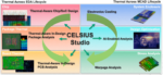
Continuing the multiphysics theme, I talked recently with Melika Roshandell (Product Management Director at Cadence) on the continuing convergence between MCAD and ECAD. You should know first that Melika has a PhD in mechanical engineering and an extensive background in thermal engineering at Broadcom and Qualcomm, all very relevant to this topic. One immediate revelation from this discussion for me was that thermal analysis and optimization for chips and systems is commonly handled by mechanical engineers working cooperatively with the electrical design teams. Makes sense, but that difference in expertise and disciplines can and often does cause significant speed bumps between these elements of design, leading to inefficiencies in execution and optimization. Celsius Studio aims to flatten these speed bumps.
A quick recap on the multiphysics need
There’s an old joke in physics. A dairy farmer asks the local university for help to understand why milk production has dropped at his farm. After hosting a tour of his farm, detailed discussions, and much study back at the university he receives a letter from the theoretical physics department. They tell him that they have found a solution, but it only works for spherical cows in a vacuum. Point being that physicists must greatly simplify a problem, prioritizing just one component to find an analytic solution.
Computer-based numerical analysis doesn’t suffer from that limitation, forgoing exact answers for approximate answers though to whatever precision is needed. It is also not limited to consider only physical effect at a time. Which is just as well because in chip and system design, multiple physical factors are significant at all levels of design and can’t be neatly separated.
Electrical activity unavoidably generates heat (second law of thermodynamics): in a transistor, a block of logic, a chip/chiplet, a package, on a board and in a rack. Heat is generated locally in areas of active usage which can lead to incorrect behavior or physical damage if not effectively dissipated. One way to reduce heating is to lower clock speeds until sufficiently cooled but that reduction also compromises performance. For optimal operation, heat generated by electrical activity (dynamic and leakage) must be dissipated passively (thermal diffusion, radiation, and convection) and/or actively (forced air or liquid cooling). Multiple types of physics must be analyzed together.
Another important consideration is the tendency of structures to warp under heating. Chips/chiplets are fabricated with multiple layers of materials, each with different thermal expansion properties. Chiplets sit on top of interposers and other layers, inside a package sitting on top of a multilayer PCB, and so on – more different materials with different expansion coefficients. When two (or more) connected layers expand under heating, one will expand more than the other. If this differential expansion is big enough the structure will warp. That adds stress to electrical connections between layers which can fracture and disconnect. Problems of this nature do not self-heal after cooling; the only way to fix your phone if connections break is to get a new phone. More multiphysics analysis is needed.
One more wrinkle makes the thermal management problem even more complex. All this analysis must work across a very wide scale range, from tens of microns in the IC design, to tens of centimeters on a board, up to meter ranges in a rack. Heat can be generated at all levels and cooling must be effective at all levels. Multiphysics analysis must also perform at multi-scale.
Celsius Studio targets comprehensive in-design analysis
Celsius Studio integrates together thermal analysis and implementation insights from Innovus for digital circuits, Virtuoso for custom/analog circuits, Integrity for 3D-ICs, AWR for microwave ICs, and Allegro for board design. These insights guide power overall thermal and stress analysis together with heat reduction strategies, placement optimization, and thermal via and temperature sensor placement.
Thermal and stress modeling are accomplished through finite element analysis (FEA), with meshes designed to support necessary accuracies from fine-grained to coarse-grained structures across that wide scale range. Heat dissipation through convection and/or through active cooling (fans, etc.) are modeled in the Cadence Celsius EC Solver.
Obviously, this analysis requires MCAD models which can be created in the tool or can be imported from multiple popular MCAD formats. Sounds easy but historically, according to Melika, difficulties in seamlessly coupling MCAD and ECAD have contributed significantly to those speed bumps. In Celsius Studio, Cadence in-house MCAD and ECAD experts have reduced the import effort from days to negligible impact on the analysis flow. Therefore providing a streamlined path to thermal, stress, and cooling analysis on boards and in-rack.
That streamlined path makes in-design analysis (IDA) a much more realistic proposition. Previous over-the-wall exchanges between engineering and thermal engineering obviously limited opportunities for co-design/optimization, tending to best guess estimates to guide thermal teams followed by a scramble at the end to align against final analytics from the electronics teams. Now with faster turn-times to import mechanical model updates, co-optimization through design becomes feasible, reducing the risk of late scrambles and schedule/BOM changes.
Comprehensive coverage without sweeping parameters
Faster turn-times also allow for AI-enabled analysis. I’m going to go out on a limb here with a little of my own speculation. To analyze/optimize a complex design with many parameters you can sweep those parameters over all possible settings and combinations. However the complexity of sweeping expands exponentially as more parameters are added. There is a concept in Design of Experiments called Covering Arrays which we have written about in an Innovation blog, to massively reduce the number of combinations you must consider while only modestly reducing coverage. There is only one problem – figuring out the right options to pick requires a lot of human ingenuity. Machine learning could be another way to get there, across many more parameters.
I don’t know if this is the method behind Optimality or other tools of this nature, but I do think some related technique may play a role. Especially since this method can be applied to any problem, mechanical or electronic, to select a small and manageable subset from an otherwise impractical sweep range, to achieve near-optimal coverage in analysis 😀
For several years now, I’ve been meeting with AMIQ EDA co-founder Cristian Amitroaie every few months to discuss the state of the industry, key trends in design and verification, and the ways that they help facilitate and accelerate chip development. I noticed an interesting new feature mentioned in their latest press release, so I asked Cristian for more information. This led to a lively and interesting discussion.
Most designers and verification engineers write their code in SystemVerilog these days, but there are exceptions. Some take advantage of high-level synthesis (HLS) tools to design in SystemC or other languages a bit more abstract than SystemVerilog. Others write in their own languages and use custom tools to generate the SystemVerilog files used for simulation, formal verification, synthesis, and other steps in the development process.
Cristian said that they occasionally see a middle ground in which engineers write code that is primarily SystemVerilog but also contains “preprocessor” statements in established languages such as Perl and Python’s Jinja2 library, or in proprietary languages. They use scripts to process these files and generate the pure SystemVerilog files for the rest of the flow. I asked Cristian how the use of preprocessors changes the way that engineers use an integrated development environment (IDE).
I learned that users of the AMIQ EDA Design and Verification Tools (DVT) IDE family want to have access to all their favorite features even when editing files with preprocessor code. The AMIQ EDA team developed clever heuristics to enable full IDE capabilities when editing such files, just as they do with pure SystemVerilog. These features include navigational hyperlinks, autocomplete, on-the-fly error detection, quick fixes, refactoring, and all the advanced functionality DVT IDE users are addicted to.
This was intriguing to me. We are talking about “understanding” mixed-language files, not really something any compiler can easily digest. To make sure I get it right and that this is for real, Cristian invited Zeljko Zurzic, the team lead who coordinated the development of this capability, to explain how it works. He said that all users need do is to inform DVT IDE about the mapping between the files containing preprocessor statements (“p file”) and the generated files (“g file”).
This is done using dedicated compiler directives that support various use cases. For example, there is a way to tell the DVT IDE compiler “go figure out the corresponding p file from the g file header comment.” Once this is done, users just edit their p files as if there is nothing special about them. On-the-fly incremental compilation will flag any SystemVerilog errors as they type, hyperlinks take them around the code, autocomplete and refactoring work just fine, they can request various diagrams, etc.
The sections that contain preprocessor code are marked distinctively so that users know they will be transformed into SystemVerilog code. In DVT Eclipse IDE they can see how code is generated by using the Inspect View; in DVT IDE for VS Code they can “peek” the transformations. DVT IDE can be configured to automatically run the preprocessing script whenever the preprocessor code is changed. Users can easily compare a p file with the corresponding g file if desired.
Zeljko provided three screenshots that show this new capability in action. The first one below shows a file in DVT Eclipse IDE that includes a Jinja2 preprocessor statement. Despite the presence of this non-SystemVerilog code, the user is able to take advantage of the powerful “Show Writers” feature to quickly understand how a variable is driven. Compilation errors and warnings are indicated in the leftmost column of the display.
The screenshot below displays the same file in DVT IDE for VS Code, showing the compiler issues in the left column and enabling the use of autocomplete. This demonstrates how even the most advanced DVT functions are available in code with preprocessor statements.
Zeljko stressed that the IDE checks the generated SystemVerilog code, important because there could be an error in a preprocessor statement or a bug in the preprocessing script. The screenshot below shows just such an example. The generated SystemVerilog code contains a variable that was not defined in the source file. DVT IDE displays the compilation error, the p file, and the generated code in the g file.
Viewing the g files can be helpful in debug, but the bottom line is that users work directly with the p files, analyzing and editing them using a powerful IDE. The g files are tagged as “read only” and users will be warned if they are modified. I was glad to hear this; we all know that it’s a really bad idea to make manual changes to any file that will be overwritten by a code generation process.
Finally, Cristian stressed that the whole point of this new feature is that users can edit code with preprocessor statements just as if it were pure SystemVerilog. Making this possible has been a significant effort driven by a few key customers who rely on preprocessor-based flows. I thanked Zeljko and Cristian for their explanations and their time.
If you’d like to learn more about using preprocessor files or any aspect of the AMIQ EDA solutions, you can visit them in Booth 107 at the Design and Verification Conference and Exhibition (DVCon) United States in San Jose, Calif. on March 5 and March 6.
Chiplets dominate semiconductor industry conversations right now – and after the recent Chiplet Summit, we expect the intensity to go up a couple of notches. One company name often heard is Blue Cheetah, and we had the opportunity to sit down with them recently to discuss their views and their just-announced design win at Tenstorrent. Their ideas on getting from chiplet specifications to chiplet ecosystems recall familiar industry dynamics with engineering and marketing working together in adoption cycles.
Two frequently-mentioned chiplet interconnect specs
Instead of a massive, complex, single-die SoC, chiplets are smaller pieces designed, fabbed, and tested independently, maybe in different process nodes, then packaged together in a bigger solution. In theory, chiplets would be reusable and interoperable. Designers could grab a chiplet without concern for what fabrication process made it or gory details we’ll see shortly, as long as the chiplet complies with a broadly adopted die-to-die (D2D) interconnect specification. Two specification candidates have bubbled to the top of the heap: BoW and UCIe.
Significant differences exist between these two specifications regarding their design philosophies, primarily driven by the types of chiplet use cases they aim to support. BoW focuses on optimizing disaggregated SoC designs with the most efficient die-to-die interconnect across a broad range of end product applications; achieving all of this requires a significant degree of flexibility in the specification. UCIe, on the other hand, focuses on plug-and-play interconnectivity and primarily aims to streamline interoperability between chiplets from any supplier.
There are some commonalities. UCIe and BoW define clock-forwarded, single-ended parallel links; this basic architecture has quickly arisen as the dominant approach for die-to-die interconnects (compared to short-reach serial link or SerDes-based approaches, which are typically differential with an embedded clock). Here are abbreviated descriptions of the two specifications – both of which have definitions suitable for either standard (organic laminate) or advanced packaging technologies:
UCIe, Universal Chiplet Interconnect Express, defining 1) a PHY layer with unit element modules whose shoreline footprint, arrangement rules, and basic structure (such as the number of signals per module) are defined based on package type, 2) a D2D adapter coordinating link states, retries, power management, and more, and 3) a protocol layer supporting CXL and PCIe traffic.
BoW defines PHY unit elements as 8- or 16-bit “slices” that can be flexibly combined and arranged to meet a given design’s bandwidth/footprint needs. Rules specify the arrangement of these slices, but the shoreline occupied by each slice, how many slices are stacked (increasing the shoreline bandwidth density, but typically requiring additional routing resources in the package), and whether/how many sideband resources to include are parameters that chiplet / chiplet interconnect designers can tailor to their needs. BoW further defines a link and transaction layer that provides error protection (via forward error correction), flow control, packetization, and, most importantly, mechanisms enabling any on-die bus/network-on-chip (NoC) protocol (and the specific versions/variants thereof) for transport by the die-to-die subsystem (link layer + PHY).
Blue Cheetah recognized early on that building efficient yet robust parallel die-to-die interfaces would require a particular set of circuit optimizations and a high degree of configurability to match the targets of any given chiplet product/design. They set out to develop a clean-sheet architecture for power, performance, area, and robustness-optimized links. Proprietary generator technology provides rapid configurability of their IP for customizing solutions to application requirements, including packaging type, data rate, orientation, I/O configuration, bus protocols/protocol variants, and more.
The decision to create efficient, configurable interconnect solutions readily adaptable for BoW or UCIe is now paying off. “We believe we have more D2D interconnect designs in flight than any other company right now,” says John Lupienski, VP of Product Engineering at Blue Cheetah. “We’re often connecting between multiple chiplet partners, which gives us an advantage in fostering collaboration.”
Accelerating adoption with chiplet ecosystems
Lupienski suggests three distinct chiplet use cases that explain what is happening in the market. The first is single vendor die disaggregation, breaking a (putatively monolithic) SoC into chiplet designs, concentrating on incremental value add where needed. Moving to a next-generation part may involve replacing only some subset of the chiplets and modifying the package. However, by definition, these are walled gardens where that one vendor controls all chiplets and all aspects of their design. (HBM memories are a notable exception in the otherwise single vendor model since they source from memory manufacturers and, as of today, are the sole exemplar of a “plug and play” chiplet.)
The use case often most discussed and implicitly or explicitly envisioned is a fluid market where firms design chiplets that interoperate flawlessly with any other vendors’ chiplets and are available to anyone. But in practice, a third use case is taking shape: chiplet ecosystems where multiple vendors jointly plan and execute chiplet product roadmaps. In contrast to the plug-and-play vision, these ecosystem chiplets are developed with more targeted scope/functionality and (typically) in partnership with other vendors participating within the same ecosystem.
Tenstorrent (helmed by Jim Keller, who has architected and/or led many highly influential processor/SoC designs) is setting up just such an ecosystem and has selected Blue Cheetah to help make it happen. SoC designers typically have an intimate understanding of how design decisions related to factors like floorplanning, subsystem partitioning, and on-die bus/NoC protocols will influence monolithic designs but might not yet have the experience to know what to consider when chiplets enter the mix.
Blue Cheetah has deep expertise and roots in chiplets. Their team includes Sehat Sutardja – credited with introducing chiplets in his 2015 ISSCC keynote – and Weili Dai as Blue Cheetah’s founding investors. Elad Alon, the company’s CEO and co-founder, is the technical lead of the BoW working group and has worked with many of the companies pioneering chiplets and chiplet ecosystems. Blue Cheetah knows what works, where the pitfalls exist, and how to help Tenstorrent and its ecosystem partners navigate AI and RISC-V chiplet design.
Navigating chiplet technology and economics
Customizable, standards-based D2D interconnects with fair-market licensing from Blue Cheetah in multiple ecosystems should make chiplets attractive to more firms. “Smaller chiplet firms going it alone face technology and economic risks while searching for critical mass,” adds Ronen Shoham, VP of Product Management at Blue Cheetah. “We’re helping create multiple ecosystems with companies including DreamBig Semiconductor, FLC Technology Group, Ventana Microsystems, and, as recently announced, Tenstorrent. The approach allows vendors to focus on capturing their core innovations as a chiplet and source other components from third parties whose expertise lies in those other areas.”
Navigators fill vital roles in technology adoption. It’s the right time for a push from those with real-world chiplet experience – we look forward to hearing more from Blue Cheetah.
– AMAT slightly better than expected, flat & guides flat but > expected
– Expects better 2024- Systems flat, service up, display down
– China risk remains high at 45%- $200M Sculpta expected in 2024
– HBM 5% of industry but not a lot of tool sales- but high growth
Still bumping along with flattish levels of business but outlook improving
AMAT reported revenues of $6.71B and EPS of $2.13 versus expectations of $6.48B and EPS of $1.91 but revenues were flat quarter over quarter and year over year. Guidance is for $6.5B +- $400M in revenues and $1.97 +- $0.18 in EPS which again is more or less flat guidance.
While AMAT positioned itself on the call as outgrowing the market in every way, the reality is flat, flat and more flat. Although there is clearly a better outlook in the industry it has not manifested itself in orders or revenues nor expected revenues.
China at 45% remains a large risk & exposure
Management believes China business will shrink over the year as a percentage of overall business. We assume that sooner or later China is running out of places to put the mountains of equipment they are buying.
The question at hand is will the eventual declines in China business be offset by increases in other markets such as memory or foundry/logic outside of China. If China slows faster than the other markets grow we will see a slower recovery.
ICAPS will be weaker in 2024
With China eventually slowing, it should come as no surprise that ICAPS (trailing edge technology) is expected to be down for 2024 as most of China’s business is more trailing edge / ICAPs business.
In our view we will eventually see a virtual Tsunami of trailing edge capacity come on line that we have dubbed the China Chipocalypse. When it will hit is unclear but it will happen. Slowing ICAPs and China business may be a leading indicator that they are chock full of equipment and may not need much more as they have built up a huge buffer of US equipment already.
This also suggests that any restrictions by the US on equipment bound for China is way too late as they already have all the equipment they need.
HBM is 5% of memory market but growing at 50% annually
Management noted on the call that HBM (high bandwidth memory) is about 5% of the memory market and growing at about a 50% rate which implies it should get to about 7.5% by end of year.
More importantly management also admitted that HBMs growth will not really translate into similar equipment growth rates as the vast majority of HBM capacity is just repurposed existing equipment and not new equipment for HBM only.
We think this is one of the biggest misunderstandings of both ignorant analysts and investors. HBM is great as it helps out the weak memory industry but it does not generate new equipment sales.
The best that HBM does for the equipment industry is soak up the excess capacity and excess equipment already existing in the field so that we will get back to better utilization sooner rather than waiting forever for growth in the standard DRAM and NAND markets.
We have repeated this many times but investors seem to ignore the reality as they are caught up in the blinding lights of the AI semiconductor frenzy. HBM is nice but its not the savior that many view it as in the semiconductor memory industry- its relatively small and doesn’t generate new equipment sales.
SCULPTA expected to be $200M in 2024
SCULPTA, the sidewall etch, NOT patterning, technology that was released through much distortion of being a double patterning ASML killer, is expected to do about $200M in revenue in 2024, which is a relative rounding error and obviously millions of miles away from having any impact on ASML’s business.
These are likely the first tools that customers will be trying out to see if it actually works as advertised. If we go back to the exaggerated hype of last year that had most analysts drinking the kool aid versus our dubious view…we clearly were right and the hype was wrong.
The Stocks
AMAT’s stock was up huge in the after market as the semiconductor frenzy continues. We would view this as a profit taking opportunity if the stock opens up anywhere near the after market pricing.
We heard a lot of flat, flat, flat and more flat but we never heard a definitive time frame for real improvements only anecdotal points of improvement that were already well baked into the stock.
Although AMAT talks a big game of out growing their peers, the real reality is that ASML has blown past AMAT to become the biggest equipment company in the world and certainly a better investment in our view.
This is not to suggest that AMAT isn’t a great company, its just that reality and hard numbers tell a different story than all the overly positive words and the frenzy of anything associated with AI that has driven the stock back into overvalued territory.
AI is certainly the greatest thing we have seen in the tech world in quite some time and perhaps the biggest thing ever but the huge impact will be on a limited number of semiconductor companies and especially Nvidia which we absolutely love (and own a lot of).
About Semiconductor Advisors LLC
Semiconductor Advisors is an RIA (a Registered Investment Advisor),
specializing in technology companies with particular emphasis on semiconductor and semiconductor equipment companies. We have been covering the space longer and been involved with more transactions than any other financial professional in the space. We provide research, consulting and advisory services on strategic and financial matters to both industry participants as well as investors. We offer expert, intelligent, balanced research and advice. Our opinions are very direct and honest and offer an unbiased view as compared to other sources.
For the 2024 SEMI International Strategy Symposium I was challenged by members of the organizing committee to look at where logic will be in ten years from a technology, economics, and sustainability perspective. The following is a discussion of my presentation.
To understand logic, I believe it is useful to understand what makes up leading edge logic devices. TechInsights produces detail footprint analysis reports, and I took reports for ten 7nm and 5nm class devices including Intel and AMD microprocessors, Apple A series and M series processors, an NVIDIA GPU, and other devices. Figure 1 illustrates what makes up the die area.
Figure 1. Logic Layouts
From figure 1 logic makes up slightly less than one half of the die area, memory slightly less that one third of the die and I/O, analog, and other the balance. I find it interesting that the SRAM memory areas actually measured is a lot smaller than the percentage I typically hear people talk about for System On a Chip (SOC) products. The plot on the bottom right shows that there is one outlier but otherwise the values are tightly clustered.
Singe logic makes up almost half the die area, it makes sense to start with the logic part of the design. Logic designs are done with standard cells and figure 2 is a plan view of a standard cell.
Figure 2. Standard Cells
The height of a standard cell is typically characterized as the Metal 2 Pitch (M2P) multiplied by the number of tracks, but looking at the right side of the figure there is a cross sectional view of the device structure that must also match the cell height and is constrained by device physics. The same is the case for the cell width that depends on the Contacted Poly Pitch (CPP) and looking at the bottom of the figure there is a cross sectional view of the device structure that once again is constrained by physics.
Figure 3 presents the result of an analysis to determine the practical limits of cell width and cell height scaling. I have a presentation that details the scaling constraints and in that presentation there are dozens of slides between figure 2 and figure 3, but with limited time I could only show the conclusion.
Figure 3. Logic Cell Scaling
Cell width scaling depends on CPP, and the left side of the figure illustrates how CPP is made up of Gate Length (Lg), Contact Width (Wc) and two Contact to Gate Spacer Thicknesses (Tsp). Lg is constrained by leakage and the minimum Lg with acceptable leakage depends on the device type. Planar devices with a single gate controlling the surface of a channel with an unconstrained thickness, is limited to approximately 30nm. FinFETs and horizontal Nanosheets (HNS) constrain the channel thickness (~5nm) and have 3 and 4 gates respectively. Finally, 2D materials introduce <1nm channel thickness, non silicon materials and can produce Lg down to ~5nm. Both Wc and Tsp have limited ability to scale due to parasitics, The bottom line is a 2D device can likely produce a ~30nm CPP versus todays CPPs that are ~50nm.
Cell height scaling is illustrated on the right side of the figure. HNS offers single nanosheet stacks in place of multiple fins. Then the evolution to stacked devices with a CFET eliminates the horizontal n-p spacing and stacks the nFet and pFET. Cell heights that are currently 150nm to 200nm can be reduced to ~50nm.
The combination of CPP and Cell Height scaling can produce transistor densities of ~1,500 million transistor per millimeter squared (MTx/mm2) versus todays <300MTx/mm2. It should be noted that 2D materials is a likely a mid to late 2030 technology so 1,500 MTx/mm2 is outside of the timing discussed here.
Figure 4 presents a summary of announced processes from Intel, Samsung, and TSMC.
Figure 4. Announced Processes
For each company and year, the device type, whether or not backside power is used, density, power and performance are displayed if available. Power and performance are relative metrics and power is not available for Intel.
In figure 4, leading performance and technology innovations are highlighted in bold. Samsung is the first to put HNS in production in 2023 where Intel won’t introduce HNS until 2024 and TSMC until 2025. Intel is the first to introduce backside power into production in 2024 and Samsung and TSMC won’t introduce it until 2026.
My analysis concludes Intel is the performance leader with i3 and maintains that status for the period illustrated, TSMC has the power lead (Intel data not available) and density leadership.
Figure 5 presents our logic roadmaps and includes projected SRAM cell sizes (more on this later).
Figure 5. Logic Roadmap
From figure 5 we expect CFETs to be introduced around 2029 providing a boost in logic density and also cutting SRAM cell sizes nearly in half (SRAM cell size scaling has virtually stopped at the leading edge). We expect logic density to reach ~757MTx/mm2 by 2034.
Both the logic transistor density projections and SRAM transistor density projections are illustrated in figure 6.
Figure 6. Transistor Density Projections
Both logic and SRAM transistor density scaling is slowing but SRAM to a greater extent and logic now has similar transistor density to SRAM.
Slide 7 summarizes TSMC data on analog scaling in comparison to Logic and SRAM. Analog and I/O scaling are both slower than logic scaling as well.
Figure 7. Analog and I/O Scaling
A possible solution to slower SRAM and analog and I/O scaling is chiplets. Chiplets can enable less expensive – more optimized processes to be utilized to make SRAM and I/O.
Figure 8. Chiplets
The figure on the right side of figure 8 comes from a 2021 paper I coauthored with Synopsys. Our conclusion was breaking apart a large SOC into chiplets could cut the cost in half even after accounting for increased packaging/assembly costs.
Figure 9 presents normalized wafer and transistor costs for logic, SRAM and I/O (please note the figure has been updated from the original presentation).
Figure 9. Cost Projections
In the right figure the normalized wafer cost is shown. The logic wafer cost are for a full metal stack that is increasing in number of metals layers. The SRAM wafers are the same nodes but limited to 4 metals layers due to the more regular layout of SRAM. The I/O wafer cost is based on a 16nm – 11 metal process. I selected 16nm to get a minimum cost FinFET node to ensure adequate I/O performance.
The figure on the right is the wafer cost converted to transistor cost. Interestingly the I/O transistor are so large that even on a low cost 16nm wafer they have the highest cost (the I/O transistor size is based on TechInsights measurements of actual I/O transistors). Logic transistor costs go up at 2nm the first TSMC HNS sheet node where the shrink is modest. We expect the shrink at 14A to be larger as a second-generation HNS node (this is similar to what TSMC did with their first FinFET node). Once again, the cost of the first CFET node also increases transistor cost for one node. SRAM transistor cost trends upward due to limited shrink except for a one time CFET shrink. The bottom line of this analysis is that transistor cost reduction will be modest although Chiplets can provide a onetime benefit.
Moving on to sustainability, figure 10 explains the different “scopes” that make up carbon footprint.
Figure 10. Carbon Footprint Scopes
Scope 1 is the direct site emissions due to process chemicals and combustion (electric can also be scope 1 if generated on-site), Scope 2 is due to the carbon footprint of purchased electricity. Scope 3 is not included in this analysis but is due to the carbon footprint of purchased materials, the use of the manufactured product and things like vehicles driven by employees of a company.
A lot of companies in the semiconductor industry are claiming that they have no carbon emission due to electricity because the electricity is all renewable. Figure 11 compares renewable to carbon free.
Figure 11. Carbon Intensity of Electricity
The key problem is that 84% of renewable energy in the semiconductor industry in 2021 was found by Greenpeace to be renewable energy certificates where a company purchases the rights to claim reductions someone else already did. This is not same as installing low carbon electric sources or paying others to provide low carbon electricity and does not in-fact lower the global carbon footprint.
Figure 12 illustrates how process chemical emissions take place and are characterized.
Figure 12. Process Chemical Emissions
Process chemicals enter a process chamber where a percentage of the chemicals are utilized in an etching or deposition reaction that breaks down the chemicals or incorporates them into a deposited film. 1-uitlization is the amount of chemical that escapes out the exhaust of the tool. The tool exhaust then may go into an abatement chamber further breaks down a percentage of the chemicals and the emissions to the atmospheres from abatement are 1-abatement. Finally, a Global Warming Potential (GWP) is applied to calculate the carbon equivalency of the emission. GWP takes into account how long the chemical persists in the atmosphere and how much heat the chemical reflects back in comparison to carbon dioxide. Carbon dioxide has a GWP of 1, semiconductor process chemicals such as SF6 and NF3 have GWP values of 24,300 and 17,400 respectively (per IPCC AR6).
Figure 13 presents some options for reducing emissions.
Figure 13. Reducing Emissions
Electricity sources such as coal produce 820 grams of CO2 equivalent emissions per kilowatt hour (gCO2e/KWh) whereas solar, hydroelectric, wind, and nuclear power produce 48, 24, 12 and 12, gCO2e/KWh respectively.
More efficient abatement systems can breakdown process gases more effectively. Fab abatement system range in efficiency from 0% for some reported US sites (no abatement) to ~90%. We estimate the worldwide 300mm fabs average is ~70% and that most 200mm and smaller wafer size fabs have no abatement. Systems with up to 99% efficiency are available.
Lower emission chemistry can also be used. Tokyo Electron has announced a new etch tool for 3D NAND that uses gases with zero GWP. Gases such as SF6 and NF3 are primarily used to deliver Fluorine (F) into chambers for cleaning, substituting F2 (GWP 0) or COF2 (GWP 1) can essentially eliminate this source of emissions.
Figure 14 illustrates a Carbon Footprint Forecast for logic.
Figure 14. Carbon Footprint Forecast
In the figure, the first bar on the left is a 3nm process run in Taiwan in 2023 assuming Taiwan’s electricity carbon footprint and 70% abatement. The second bar is a 5A process and the emission that would result if the same 2023 Taiwan electricity carbon intensity and 70% abatement were used. The increase in process complexity would drive up the overall footprint by 1.26x. Looking forward to 2034 Taiwan’s electricity is expected to decarbonize significantly, also 90% abatement should be common, and the third bar shows what a 5A process would look like under this condition. While this represents cutting emissions by more than half, growth in the number of wafers run by the industry for 2034 would likely overwhelm this improvement. The final bar on the right is what is possible with sufficient investment, it is based on low carbon electricity, 99% abatement, and using F2 for chamber cleaning.
Figure 15 presents our conclusions:
Figure 15. Conclusion.
Transistor density, and wafer and die cost estimates were generated using the TechInsights Strategic Cost and Price Model, an industry roadmap that produces cost and price estimates as well as detailed equipment and materials requirements. The GHG emission estimates were produced using the TechInsights Semiconductor Manufacturing Carbon Model. For more information, please contact sales@techinsights.com
I would like to acknowledge my colleagues in the Reverse Engineering Business Unit at TechInsights, their digital floorplan and process reports were very helpful in creating this presentation. Also, Alexandra Noguera at TechInsights for extracting I/O transistor sizing data for this work.