
Heat and semiconductor reliability exist in an inversely proportional relationship. Before the breaking point at the thermal junction temperature rating, every 10°C rise in steady-state temperature cuts predicted MOSFET life in half. Yet, heat densities rise as devices plunge into harsher environments like smartphones, automotive electronics, and space-based electronics, while reliability expectations remain high. Higher frequencies and increased power delivery with newer semiconductor materials and packaging schemes push thermal behavior harder. Accurate reliability prediction is only possible with advanced electro-thermal simulation – an emphasis for several Keysight teams working with PathWave Advanced Design System (ADS).
Keysight’s advanced thermal analysis capability stretches back to its acquisition of Gradient Design Automation and its HeatWave thermal solver in 2014. ADS Electro-Thermal Simulation adapted and integrated HeatWave to co-simulate with industry-leading RF circuit simulators in ADS. Gradient’s former VP of Engineering, Adi Srinivasan, now a Product Owner and Principal Engineer for electro-thermal simulation at Keysight, still works with the technology he helped pioneer today. “Coupling is now at least as important as self-heating,” says Srinivasan, and like EM simulation, the co-simulation must span time and frequency domains.
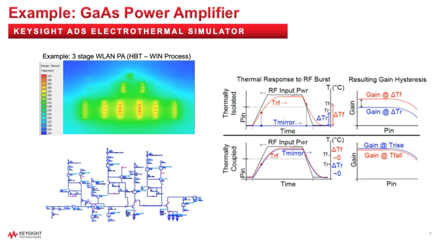
RF designers widely use ADS Electro-Thermal Simulator to avoid thermal hazards and improve design quality, with a long history of solving complex RF intra-die thermal problems. A PCB-level thermal solver, PE-Thermal, is creating similar problem-solving opportunities for power electronics designers. Increasing the reach of thermal simulation for more customers and larger domains like modules is a priority; thermal modeling in foundry process design kits (PDKs) is a strong driver of broader adoption.

III-V and silicon foundries picking up the thermal pace
Foundries are seeing increased demand for rich-model PDKs as customers crank up more simulations in their EDA workflows. Behind the scenes, Keysight has been working aggressively to evangelize the need for advanced electro-thermal simulation and asking foundries to consider adding thermal models ready for the W3050E PathWave ADS Electro-thermal Simulator to their PDK support.

“We’ve recently seen thermal-enabled PDK announcements from III-V foundries like GCS (Global Communication Semiconductors) in the US, and AWSC (Advanced Wireless Semiconductor) and Wavetek in Taiwan,” says Kevin Dhawan, III-V Foundry Program Manager at Keysight. These foundries are leaders in technology used in power and RF electronics, and Dhawan noted that other III-V foundries such as WIN, UMS, and OMMIC also offer PDKs for ADS Electro-Thermal Simulator. Additionally, Dhawan says several high-volume silicon foundries have PDK support for ADS Electro-Thermal Simulator but have yet to make specific announcements.
“Customers are asking about a single solution for both EM and electro-thermal effects, but the domains are a bit different,” Dhawan observes. “EM focuses more on back-end layout, metallization, and bias, while electro-thermal needs to model additional heat from the semiconductor devices themselves.” ADS supports several types of PDKs: ADS-native PDKs, ADS-Virtuoso interoperable PDKs, and interoperable PDKs (iPDKs) based on OpenAccess and customizable via Python and Tcl. Dhawan says to check with the foundries for the latest on ADS Electro-Thermal Simulator-ready PDKs.
Incredible heat densities in power electronics
Power converter designers are chasing extremely dense “bricks” for applications like aerospace, automotive, and device chargers. This chart shows why more designers are turning to III-V processes like GaN and SiC – switching speeds are higher, and power delivery increases.

“With tens of kilowatts or more in play, things tend to heat up,” says Steven Lee, Power Electronics Product Manager for Keysight EDA. “Traditional workflows and tools like Spice don’t consider detailed temperature profiles or post-layout thermal impacts.” The result often is a hardware prototyping surprise, where measurements find power transistors pushed beyond their rated junction temperature, triggering an expensive late part change and a re-spin.
Thermal simulation, taking device models, packaging, and board materials and layout into consideration, prevents problems. “Hot transistors next to each other can couple via metal traces and planes and magnify heating problems,” Lee points out. First-pass thermal effects discovered quickly via simulations can validate component selection and guide packaging and layout adjustments before committing to hardware.

PE-Thermal implements a thermal resistance editor and extraction tool for more robust temperature modeling capability. “With a design already in the ADS workspace, designers can select the components for thermal analysis, tune models as necessary, and simulate with PE-Thermal in a few minutes,” explains Uday Ramalingam, R&D engineer at Keysight. “Ultimately, designers will be able to go inside a transistor and explore package properties – maybe they have the right part but not the right package for their context.”

“Just like the EM solver in ADS takes metallization into account, the electro-thermal solver does too, and enhancements in future ADS releases will take us all the way to complete board-level layout thermal effects automatically,” Lee wraps up.
An RF design example of advanced electro-thermal simulation
Reliability prediction tools are only as good as the temperature data that goes into them. Excruciating setups can get accurate temperature measurements on physical hardware, but they slow design cycles and don’t preclude the re-spin surprise if bad results appear.
EnSilica (Abingdon, UK) is a fabless chipmaker delivering RF, mmWave, mixed-signal, and high-speed digital designs for their customers in automotive, communications, and other applications. Using Keysight PathWave ADS and PathWave ADS Electro-Thermal Simulator is taking them from a practice of embedding and measuring many temperature sensors on a chip to fully simulating thermal effects with high accuracy.
A Ka-band transceiver project, implemented in an automotive-certified 40nm CMOS foundry process, is EnSilica’s first foray into virtual thermal analysis. An interesting wrinkle is another chip on their board, next to the RF transceiver, creating 3°C boundary heating on one edge, clearly seen on the right side of the heat map produced in the ADS Electro-Thermal Simulator.

Results from the ADS electro-thermal simulation were within 0.7°C of actual measurements (with simulations slightly higher, an excellent conservative result), increasing confidence in meeting 10-year reliability goals. During thermal resistance modeling, EnSilica also found improvements in chip layout and package bumping that lowered operating temperatures in the final product.
Seeing deeper inside chips to avoid design hazards and enhance packages and layouts are powerful justifications for advanced electro-thermal simulation. Keysight’s ability to fit into multi-vendor workflows means high-accuracy thermal analysis is available to more design teams. Please visit these resources for the EnSIlica case study and further background on Keysight’s ADS solutions, including ADS Electro-Thermal Simulator.
Design and simulation environment: PathWave Advanced Design System
Thermal simulation add-on: W3050E PathWave Electro-Thermal Simulator
Webinar: Using Electro-Thermal Simulation in Your Next IC Design
Video: Using Electro-Thermal Simulation in ADS 2023
Case study: Predicting Ka-band Transceiver Thermal Margins, Wear, and Lifespan
Share this post via:


Comments
There are no comments yet.
You must register or log in to view/post comments.