
To create quantum computing chips today, a typical designer must cobble various tools together, switching back and forth between them for different tasks. By contrast, EDA solutions such as Keysight Advanced Design System (ADS) unify a design workflow in a single interface with automated data exchange between features. In an industry-first, Keysight QuantumPro brings five different functions for quantum design together in a superconducting qubit design workflow, reducing design cycle time and prototyping and yield risk for optimized quantum chips. Keysight’s Quantum EDA solution focuses on accurate electromagnetic modeling, ensuring that simulation and measurement outcomes align effectively.
Adding superconducting qubits presents a yield challenge
Superconducting quantum computers rely on qubits constructed from Josephson junctions held at cryogenic temperatures, which exhibit non-linear inductance needed in constructing two-level systems. Qubits interconnect by meander line coplanar waveguide resonators with frequencies often in the 4 to 10 GHz range. The resonators serve two primary functions: indirectly reading out the state of the qubits and entangling them with each other. Quantum amplifiers with gain and unique ultra-low noise characteristics amplify the output signal from qubits to improve the readout fidelity. Quantum processing units (QPUs), comprising arrays of qubits and resonators, are positioned to showcase quantum advantage, surpassing the reach of classical CPUs.
The advantage of quantum computing arises from its distinct exponential increase in computational capacity as the number of entangled qubits grows, with n qubits taking on 2n stable states. Scaling the number of qubits in quantum computing presents a formidable challenge, with the stability and coherence of qubits becoming more complex with each addition. By tying four design themes – structural layout, electromagnetic analysis, complex quantum circuit optimization, and system-level exploration and troubleshooting – into a single quantum design workflow, designers can thoroughly exercise every part of a design, make data-based adjustments, and re-simulate to verify improvements.

Unlike digital circuit design, the challenge of designing quantum chips is more than step and replication. For entanglement to work correctly, resonance frequencies must be unique within and between all nearby qubits. If two (or more) resonance frequencies overlap, qubits entangle improperly due to unpredictable cross-coupling, and the quantum chip becomes a yield failure. Factors such as minimizing environmental interference, maintaining qubit entanglement, and managing errors due to decoherence pose significant obstacles. Debugging problems discovered after fabricating chips and cryogenic testing become expensive and time-consuming.
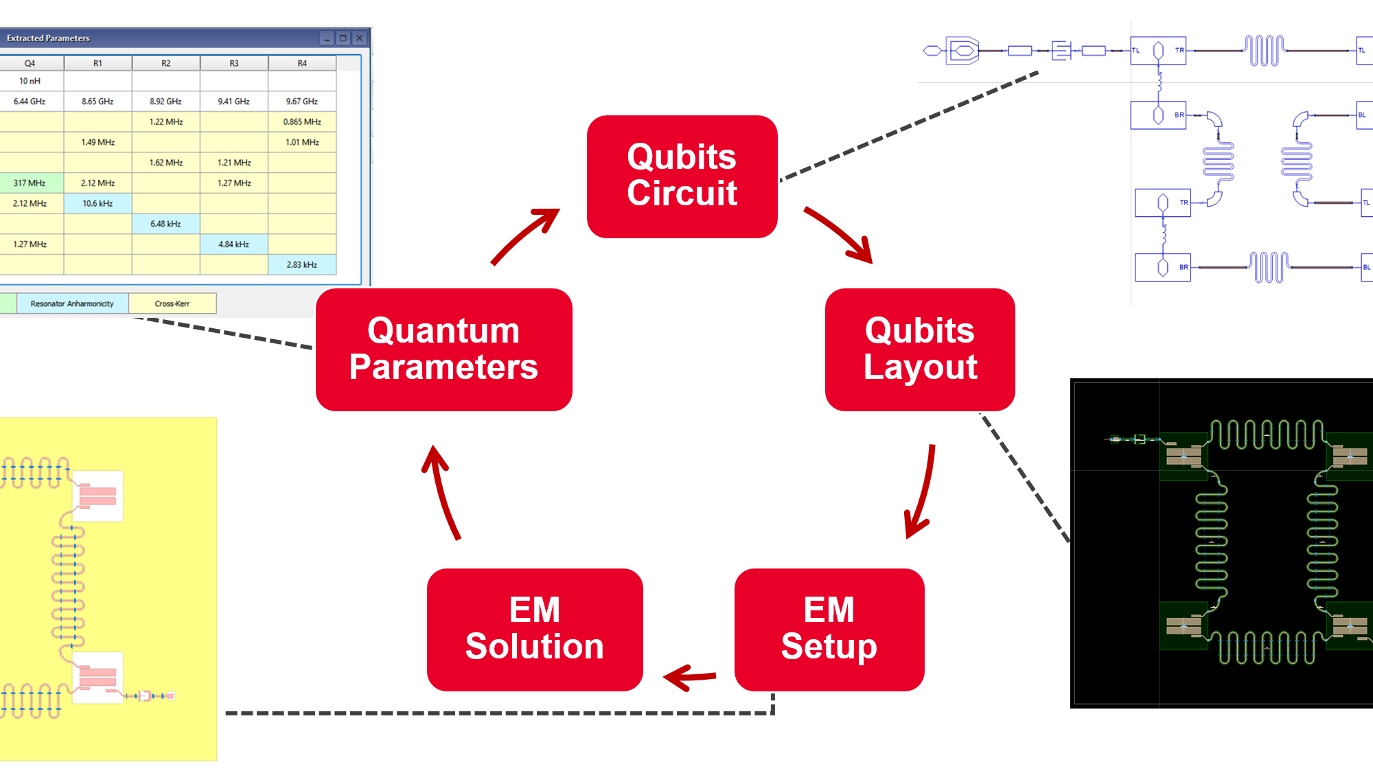
Enabling a five-point superconducting qubit design workflow
A better solution is a shift left for quantum chip design – integrating layout and simulation tools to predict and optimize resonance frequencies accurately in virtual space. RF designers are familiar with these workflows, but quantum designers are just beginning their adoption. “QuantumPro bridges the gap from ad-hoc quantum chip design with inherent yield risks to confidence in layout and simulation for predictable parts,” says Mohamed Hassan, Quantum Solutions Planning Lead at Keysight.

QuantumPro integrates five functions built on the ADS platform to streamline superconducting qubit designs, including schematic design, layout creation, electromagnetic (EM) analysis, non-linear circuit simulation, and quantum parameter extraction. Beginning with the schematic interface, users can effortlessly drag and drop components from the built-in quantum artwork. Subsequently, a layout can be generated automatically from the schematic.
Within QuantumPro, two distinct analyses are available. First, the Full EM Analysis facilitates a frequency sweep of circuits, producing s-parameters at input and output ports. The platform supports both the finite element method (FEM) and the method of moments (MoM) for the Full EM analysis. Second, the Energy Participation Analysis allows for finding the eigenmodes of the system with the FEM solver. Instead of solving for the electric field over the entire volume, the MoM solves only for the currents on the metal surface, significantly cutting computational costs.
Quantum parameter extraction is automatic in QuantumPro, with quasi-static, black box quantization, and energy participation ratio (EPR) methods. A simplified layout of a four-qubit design shows the transmon qubits (Q1 through Q4) and meander line resonators (R1 through R4). Note the unique resonance frequency values extracted by each of the three different methods in QuantumPro.

EM simulation of superconducting qubits requires one extra step. Superconductors exhibit kinetic inductance, an additional inductance large enough to sway results compared with perfect electric conductors. “Designers can’t ignore kinetic inductance – it can cause a miss in resonance frequency by as much as 40% in some cases of thin film superconductors,” says Hassan. Superconductor material editors in ADS and EMPro allow designers to describe materials for accurate kinetic inductance capture.
A core feature from ADS in QuantumPro is a Python console that gives users more control over workspaces and user interfaces and the ability to script and automate repetitive tasks.
Scaling quantum chips to hundreds or thousands of qubits
QuantumPro assures superconducting quantum chip designers get the results they expect at prototyping after simulation and optimization of designs. QuantumPro arrives at a pivotal point in quantum computing development as designers seek to move from designs with tens of qubits into the hundreds and perhaps thousands. As in conventional semiconductors, reducing prototype re-spins and improving yields can help move ideas from research to commercialization more quickly.
Designers will also see a productivity boost in their superconducting qubit design workflow with QuantumPro, which may also lower the learning curve for designers from other disciplines. Resources on the Keysight website explain more about the science behind superconducting qubits and the EM analysis and parameter extraction methods in QuantumPro.
QuantumPro webpages, with links to an application note, technical overview, and videos:
Quantum EDA: Faster design cycles of superconducting qubits
Share this post via:


Comments
There are no comments yet.
You must register or log in to view/post comments.